International Journal of Advanced Research in Electrical, Electronics and Instrumentation Engineering
ISSN ONLINE(2278-8875) PRINT (2320-3765)
ISSN ONLINE(2278-8875) PRINT (2320-3765)
Susmrita Srivastava1, Naresh Kumar Chaudhary 2 and SachchidaNand Shukla3
|
| Related article at Pubmed, Scholar Google |
Visit for more related articles at International Journal of Advanced Research in Electrical, Electronics and Instrumentation Engineering
A new circuit model of a small-signal narrow-band amplifier is proposed and analyzed on the qualitative scale. Proposed amplifier uses two MOSFETs and a BJT in Triple Darlington configuration with two additional biasing resistances in the circuit. With low distortion percentage (1.28%), the proposed circuit successfully amplifies small-signals of 1-10mV range and simultaneously provides high voltage gain (311.593) and current gain (13.971K) with narrow bandwidth (9.665KHz). Variations of maximum voltage gain with different biasing resistances and DC supply voltage and the temperature sensitivity of various performance parameters are elaborately studied and discussed in length. Qualitative performance of the proposed amplifier is also compared with the circuit which is having BJT-MOSFET in Darlington pair configuration. The proposed amplifier can be used to process audio range signal excursions and may be useful for those applications where high voltage and current gain would be the prime requirement of amplification in narrow-band low frequency region.
Keywords |
| Small-signal amplifiers, Common Source MOS amplifiers, Triple Darlington amplifiers, MOSFET Darlington pairs |
INTRODUCTION |
| Output signals from most of the electronic systems (e.g. analog, digital, or a hybrid combination of analog and digital) are often too small in magnitude to be processed reliably for executing any useful function [1]-[3]. Thus, most of these systems require amplifiers for scaling signals to a useful level [1]-[3]. |
| A Darlington pair, which is basically a composite unit of two similar transistors, has effectively proved its importance to amplify small signals [1], [3]-[7]. It has superior characteristics regarding current gain but a major drawback is encountered with its performance. At higher frequencies its response becomes poorer than that of a single transistor amplifier [3]-[7]. Numerous modifications are attempted in Darlington pair amplifiers to overcome this problem [8]-[12]. Some of the popular attempts are- the use of dissimilar active devices or hybrid combination of active devices in Darlington pair or in Triple Darlington topology and the use of some additional biasing resistances in respective amplifier circuits [8]-[12]. |
| The present investigation is focused around a compound unit which uses two identical MOSFETs and a BJT in ‘Triple Darlington topology’ [3], [6], [9]. Though the MOSFETs are suitable for developing high speed switching circuits, memory segments, logic gates, buffer amplifiers, power amplifiers and trans-conductance amplifiers [13]-[14] but in the present exploration a MOSFET dominant Triple Darlington structure with appropriate biasing components is explored as new circuit model of a small-signal amplifier. This amplifier may be suitable for those applications where high voltage and current gain would be the prime requirement of amplification in narrow-band low frequency region. Dependency of qualitative performance of the proposed amplifier on various biasing parameters, biasing supply and operational frequency is analyzed and also compared with a high voltage gain small-signal amplifier that uses MOSFET and BJT in Darlington pair [15]. |
II. CIRCUIT DESCRIPTION |
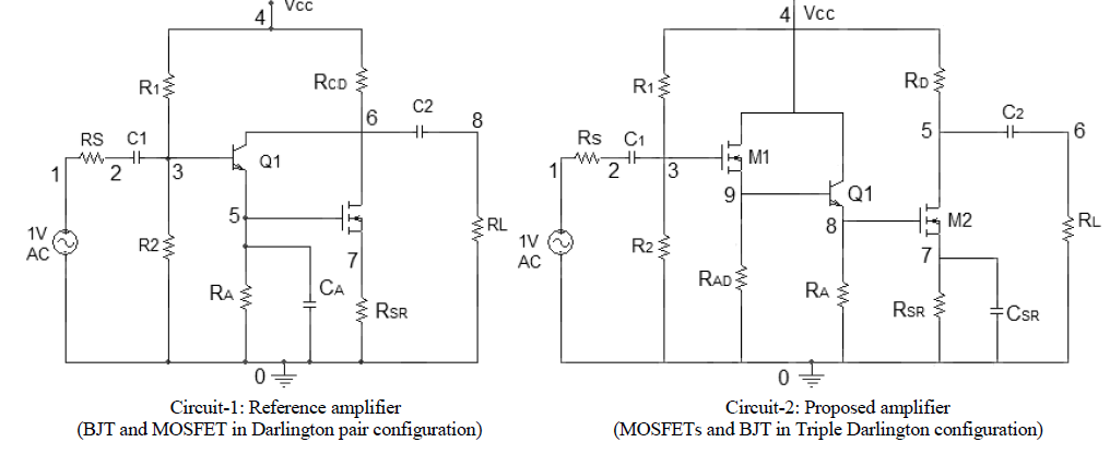
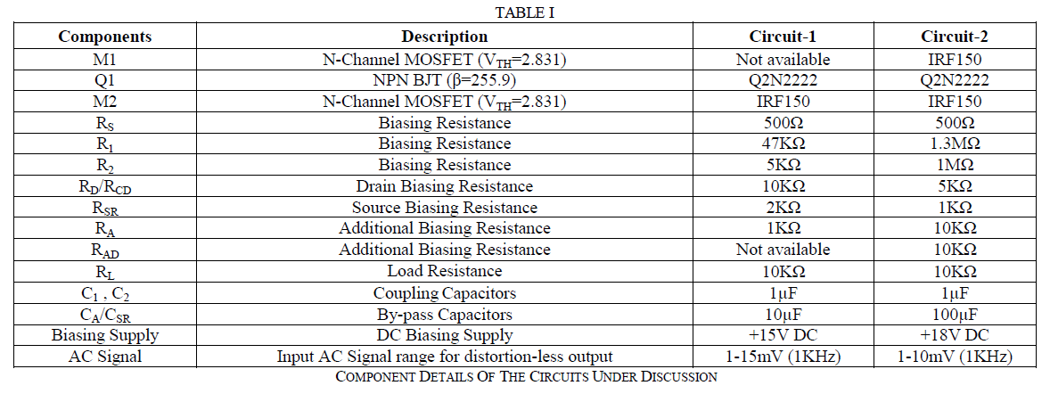
| The present work comprises a qualitative comparison between Circuit-1 [15] and Circuit-2 amplifiers. Circuit-1 amplifier, which is stated herein ‘Reference Amplifier’ [15], consists a compound unit of BJT and MOSFET in Darlington pair configuration with an additional biasing resistance RA in the circuit. However, Circuit-2 amplifier, which is termed as ‘Proposed Amplifier’ in the manuscript consists two identical MOSFETs and a BJT in Triple Darlington configuration. Unlike reference amplifier, the drain point of M1 and collector point of Q1 in proposed amplifier are directly connected to the biasing supply VCC. In addition, two additional biasing resistances RA and RAD are introduced in the proposed circuit with bypass capacitor across the source resistance. Both the amplifier circuits are properly biased using potential divider network with biasing parameters as described in TABLE I. |
| Reference amplifier [15] is biased with +15V whereas proposed amplifier is biased with +18V DC power supply. PSpice simulation (Student version 9.2) is performed to carry out present investigations [16]. Observations are procured by feeding the respective amplifier circuits with 1V AC input signal source, from which, a small-distortion-less AC signal of 1mV at 1KHz frequency is drawn as input for the amplification purpose. |
 |
 |
III. RESULTS AND DISCUSSIONS |
| The amplifier of Circuit-1 [15] provides fair and distortion-less results for 1-15mV AC input signals whereas amplifier of Circuit-2 provides the same for 1-10mV. |
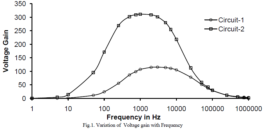
| Variation of maximum voltage gain as a function of frequency for both the amplifiers is depicted in Fig.1. The reference amplifier of Circuit-1 [15] produces 115.522 maximum voltage gain AVG (with 106.607mV peak output voltage VOP), 35.242 maximum current gain AIG (with 10.661μA peak output current IOP) and 22.258KHz bandwidth (with lower cut-off frequency fL=443.567Hz and upper cut-off frequency fH=22.702KHz) whereas the proposed amplifier of Circuit-2 produces 311.593 maximum voltage gain VAG (with 314.923mV VOP), 13.971K maximum current gain IAG (with 31.494μA IOP) and 9.665KHz bandwidth (with fL=151.056Hz and fH=9.817KHz). Clearly, the proposed amplifier produces higher voltage and current gain on the cost of reduced bandwidth. |
| In fact polarity of Darlington’s unit is determined by the driver device [17]. For example, a paired unit consisting BJT as driver and MOSFET as follower device (as in Circuit-1) principally behaves like a BJT dominating Darlington unit [11]-[12], [17]. Thus, due to driver MOSFET, the overall behaviour of the compound unit in proposed amplifier seems to be inclined more towards MOSFET and motivates respective circuit to produce extra ordinarily high current gain [11]-[12], [17]. However, considerably high voltage gain of the proposed amplifier is perhaps due to the presence of hybrid combination of MOSFETs and BJT along with two additional biasing resistances in the circuit configuration. |
 |
| In addition, both the amplifiers show phase reversal in respective output waveforms [10]-[12], [15], [17]. In fact, CE and CS configurations of the respective devices independently produce phase reversal in their output waveforms. Phase switching property of the independent active devices is responsible to produce 180o phase difference in the output waveform of reference and proposed amplifiers which are using compound unit of BJT-MOSFET and MOSFET- BJT-MOSFET in their circuit configurations [10]-[12], [15], [17]. |
| It is also worth mentioning that both the amplifiers effectively remove the problem of poor response of conventional Darlington pair or Triple Darlington amplifiers at higher order frequencies in the prescribed frequency-response range [6]-[9], [10]-[12], [15], [17]. |
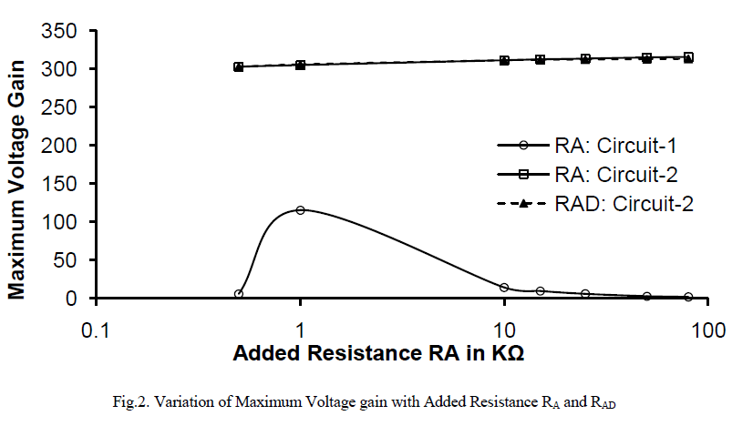 |
| Dependency of maximum voltage gain on additional biasing resistances RA and RAD for reference and proposed amplifiers is depicted in Fig.2. Both the amplifiers do not show any response for RA<0.5KΩ [15]. Corresponding voltage gain for Circuit-1 amplifier founds its maximum at RA=1KΩ, thereafter, it decreases almost exponentially at elevated values of RA [15]. However for amplifier of Circuit-2, the AVG increases only a bit at increasing values of RA and RAD and finally acquires a state of saturation beyond 50KΩ. Corresponding curves suggest that the proposed amplifier shows almost similar response for RA and RAD in terms of voltage gain. In addition, respective voltage and current gains for the reference amplifier without RA and for the proposed amplifier without RA and/or RAD dips below unity. Thus, the presence of RA and/or RAD in respective amplifiers is essential to maintain the high voltage and current gain features. |
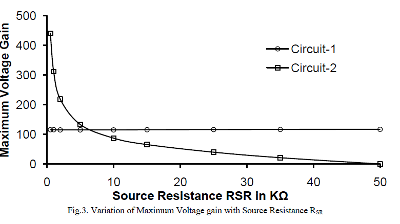 |
| Variation of maximum voltage gain AVG with Source resistance is shown in Fig.3. For reference amplifier, the increasing values of source resistance RSR barely affect the voltage gain [15]. If RSR is removed from Circuit-1, corresponding values of AVG, AIG and THD rises fractionally to 115.872, 35.288 and 3.50% respectively whereas bandwidth reduces to 21.458 KHz (with fL=449.388Hz and fH=21.908KHz). Thus, the removal of RSR from reference amplifier Circuit-1 hardly affects the performance of amplifier [15]. However, AVG of the proposed amplifier found its maximum at RSR=0.5KΩ, thereafter, it decreases almost exponentially to reach below unity at 50KΩ. Though the voltage gain of proposed amplifier reaches to maximum at 0.5KΩ of RSR but it limits the performance of the circuit to 1-4mV input AC signal. Since the resistance RSR in the proposed amplifier circuit behaves as source resistance for MOS driven composite unit therefore the source degeneration property of common source MOSFET amplifier forces voltage gain to fall almost exponentially with RSR (Fig.3). |
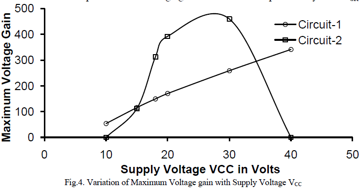 |
| Variation of maximum voltage gain AVG with DC supply voltage VCC is depicted in Fig.4. Voltage gain of the reference amplifier rises almost linearly at increasing values of VCC but for proposed amplifier it increases non-linearly from 10V to 30V of VCC, thereafter, drops to a lowest point at VCC=40V [15]. The permissible range for the reproduction of the amplified output at different VCC for reference amplifiers (Circuit-1) is 10-40V whereas this range is substantially reduced to 15-30V for proposed amplifier. This is perhaps due to MOSFET driven Triple Darlington unit of the proposed amplifier which bears a threshold voltage of 2.831V along with a high driving voltage at node 3. This driving voltage (at node 3) increases with VCC and reaches to 13.045V at 30V of VCC. This simply means that the MOSFET conducts for a driving voltage range of 2.831-13.045V corresponding to 10-30 volts of VCC. As VCC increases beyond 30V, the compound unit receives a better flow of electrons from source to drain. VCC exerts a heavy attractive force on electrons entering the drain from the channel region [14]. So beyond VCC >30V, the drain absorbs more electrons than the channel could supply. As a result, the channel completely pinches-off and thus subsequent increase in VCC>30V has minor effect on output voltage [14]. This caused the voltage gain to be rolled-off. |
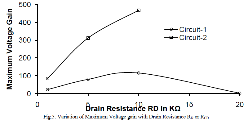 |
| Maximum voltage gain highly depends on drain resistance [10], [13]-[15]. Its variation with RCD or RD is depicted in Fig.5. For reference amplifier, the voltage gain gradually increases with RCD and attains maxima at RCD=10KΩ, thereafter, falls down rapidly and produces a distorted output beyond 20KΩ. However, for proposed amplifier, the voltage gain increases with RD and attains a maximum at RD=10KΩ, thereafter, the circuit starts producing a distorted output. |
| Variation of maximum voltage gain with load resistance RL is also studied for both the amplifiers under discussion (but not shown in form of graphs). It is observed that the voltage gain gradually rises up to 100KΩ value of RL for both the amplifiers and then tends toward a saturation tendency at higher RL. This rising and saturation of the voltage gain with RL is found well in accordance of the usual behaviour of small signal amplifiers [2], [4]-[15]. |
| Total Harmonic Distortion (THD) percentage for both the amplifiers under discussion is also calculated using established rules [10]-[12], [17]. Reference amplifier holds 3.48% THD for 8 significant harmonic terms whereas proposed amplifier shows only 1.28% THD for 10 significant harmonic terms [15]. In fact, MOS driven composite unit of the proposed amplifier virtually acquires the property of a MOSFET. The fast switching property of this virtually behaved MOS composite unit perhaps reduces the propogation delay between positive and negative half cycles of the output waveform. This decreases the distortion in output waveform and causes THD of the proposed amplifier to reduce to a significant limit. |
| During the course of qualitative analysis of the proposed amplifier, some interesting observations are received. When the biasing resistance R1 and/or R2 is removed from Circuit-2, the respective amplifier doesn’t behave properly. Similarly, when drain of MOSFET M1, of the proposed amplifier is detached from VCC (node-4) and connected to node-5, the voltage gain falls to 265.586, bandwidth to 1.737KHz and current gain to 3.25K whereas THD increases to 4.23%. However, when collector of BJT Q1 of the proposed amplifier is detached from VCC (node-4) and connected to node-5, the voltage gain falls to 282.977, bandwidth raised to 11.515KHz and current gain drops to 12.879K whereas THD reduces to 1.07%. Moreover, if M1 and Q1 of the proposed amplifier are simultaneously removed from VCC and connected to node-5, the voltage gain falls to 243.745, bandwidth to 1.836KHz and current gain to 3.113K whereas THD increases to 4.18%. |
| Variation of voltage gain, current gain and bandwidth with temperature is also measured and listed in TABLE II. Voltage gain and bandwidth gradually decreases whereas current gain increases throughout the rising temperature for reference amplifier [15]. However, for proposed amplifier, voltage gain, current gain and bandwidth decreases with rising temperature. In fact, the mobility of majority carriers of the semiconductor decreases at elevated temperature due to higher collision rate between them and the ions [18]. This decreases the drain current and therefore the current and voltage gains of the proposed amplifier. Similarly, effective contribution to the source capacitance due to the presence of Triple Darlington compound unit increases with increasing temperature [19] which in turn reduces the bandwidth. |
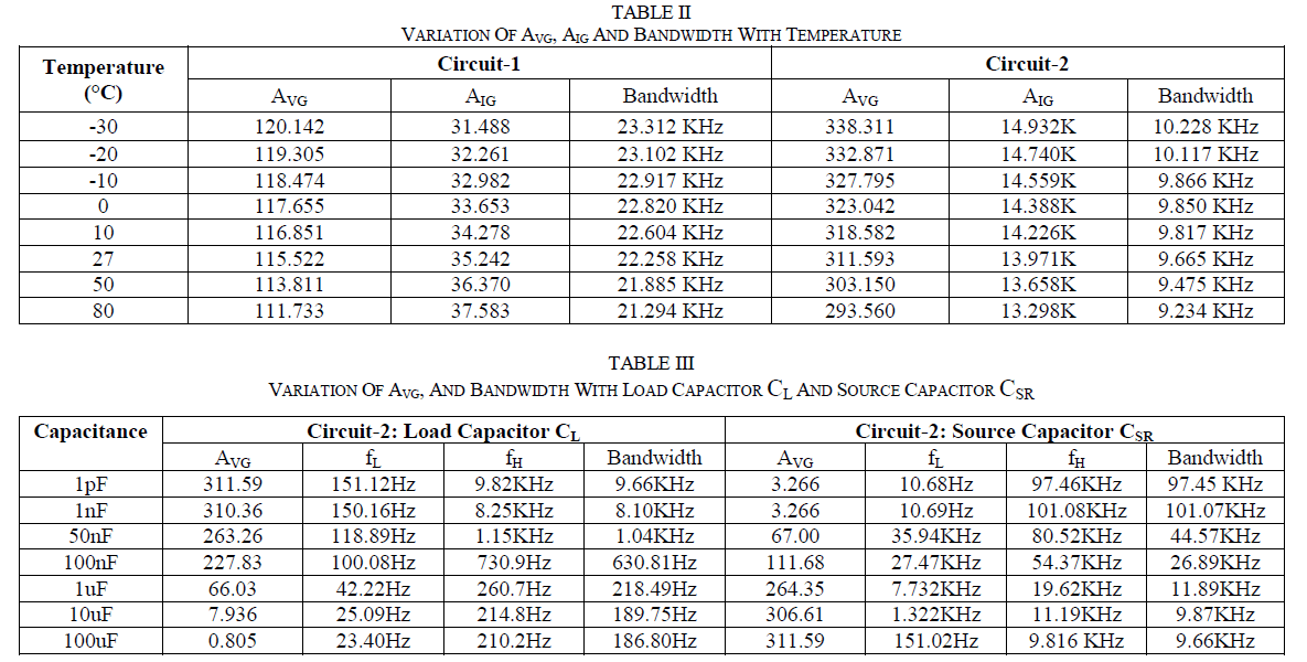 |
| Load capacitor CL (physically not shown in Circuit-2) and source capacitor CSR considerably affects the performance of proposed amplifier [14]. TABLE III comprises the variation of AVG, AIG and Bandwith with CL and CSR respectively. The maximum voltage gain AVG reduces appreciably if load capacitor CL is large. Similarly, lowering the value of CL causes midband frequency range to get wider. In addition, lower and upper cut-off frequencies shift towards lower side on the frequency scale at elevated values of CL [14]. However, as source capacitance CSR is increased, the voltage gain of the proposed amplifier increases but bandwidth decreases [14]. Moreover, shifting of lower and upper cut-off frequencies towards low frequency side on the similar pattern as was observed for CL. |
IV. CONCLUSIONS |
| A Triple Darlington configuration with two MOSFETs and a BJT is used to explore a new circuit model of RC coupled small-signal amplifier. This amplifier can effectively process small-signals swinging in 1- 10mV range of input signal at 1KHz frequency and is also free from the problem of poor response of small-signal Darlington pair or Triple Darlington amplifiers at higher frequencies. With narrow range bandwidth, the proposed amplifier generates only 1.28% harmonic distortion and simultaneously produces high voltage and current gains. Presence of load capacitor CL and source capacitor CSR considerably affects the performance of proposed amplifier whereas high voltage as well as current gain logically sets its power gain greater than unity. Presence of additional biasing resistances RA and/or RAD in proposed amplifier is essential to maintain its high voltage and high current gain features. The proposed amplifier produces 180o phase shifted output with an optimal performance for 15-30V DC supply voltage. Collectively, these features make the proposed circuit fabulously unique in the category of small-signal amplifiers based on Darlington’s topology. |
ACKNOWLEDGMENT |
| Authors gratefully acknowledge the facilities provided by the Department of Physics and Electronics, Dr. Ram Manohar Lohia Avadh University, Faizabad, U.P., India for the present investigations. Authors would also like to thank to other workers of the research group for their valuable suggestions and support during the development of present manuscript. |
References |
|