International Journal of Advanced Research in Electrical, Electronics and Instrumentation Engineering
ISSN ONLINE(2278-8875) PRINT (2320-3765)
ISSN ONLINE(2278-8875) PRINT (2320-3765)
SachchidaNand Shukla1 and Susmrita Srivastava2
|
| Corresponding Author: SachchidaNand Shukla, E-mail: sachida_shukla@yahoo.co.in |
| Related article at Pubmed, Scholar Google |
Visit for more related articles at International Journal of Advanced Research in Electrical, Electronics and Instrumentation Engineering
A new circuit model of a small-signal amplifier is proposed and analyzed on the qualitative scale. Apart from routine biasing components, the proposed amplifier circuit uses two additional biasing resistances and three dissimilar active devices namely MOSFET, JFET and BJT in Triple Darlington configuration. Having a considerably low amount of distortion (0.71%), the proposed circuit successfully amplifies small-signals of 1-5mV range (at 1 KHz frequency) and simultaneously provides high voltage gain (189.846) and high current gain (16.542K) with moderate range bandwidth (369.529KHz). These properties offer a flexible application range to the proposed circuit as high voltage gain or high current gain or high power gain amplifier in permissible audio-frequency range. Variations in voltage gain as a function of frequency and different biasing resistances, temperature dependency of performance parameters, bandwidth and total harmonic distortion of the amplifier are perused to provide a wide spectrum to the qualitative studies. Qualitative performance of the proposed amplifier is also compared with two different circuits which are respectively having BJT-JFET and BJT-MOSFET in Darlington pair configuration. The proposed amplifier may be useful for those applications where high voltage and current gain would be the prime requirement of amplification in audio frequency region.
Keywords |
| Small-signal amplifiers, Darlington amplifiers, Compound configurations, Triple Darlington configuration |
INTRODUCTION |
| One of the important concepts in electronics is the process of amplification through various active devices [1]-[2]. Virtually most of the electronic systems (analog, digital, or a hybrid combination of analog and digital) require amplifiers for scaling signals to a useful level [1]-[3]. The output signals from these systems are often too small in magnitude to be processed reliably for executing any useful function [2]-[4]. A Darlington pair, which is basically a composite unit of two similar transistors, can successfully amplify these signals [1]-[7]. It has superior characteristics regarding current gain due to which it is generally employed for the design of output stages in operational amplifiers [3]-[4]. However, a major drawback is encountered with its performance. At higher frequencies its response becomes poorer than that of a single transistor amplifier [3]-[7]. To overcome this problem, a number of modifications are attempted in Darlington pair amplifiers either by adding some extra biasing resistances in the circuit or by using Triple Darlington topology [5], [7]-[10]. However, use of dissimilar active devices or hybrid combination of active devices in Darlington’s topology is still an area of electronic circuit designers to work with [8], [11]-[12]. |
| The present investigation is focused around the use of a hybrid combination of MOSFET, JFET and BJT in Triple Darlington topology. This configuration with two additional biasing resistances is explored as new circuit model of a small-signal amplifier. The proposed amplifier circuit can be used in those radio and TV receiver stages which require high voltage gain, high current gain and moderate range bandwidth as a prime feature. |
| The present exploration is described in four sections. Section I gives the preface and the idea behind the present findings. Section II describes the detail of circuit configuration of the amplifiers under discussion. Section III contains the observational details and related discussions whereas the last section IV concludes the proposed work followed by references. |
II. EXPERIMENTAL CIRCUITS |
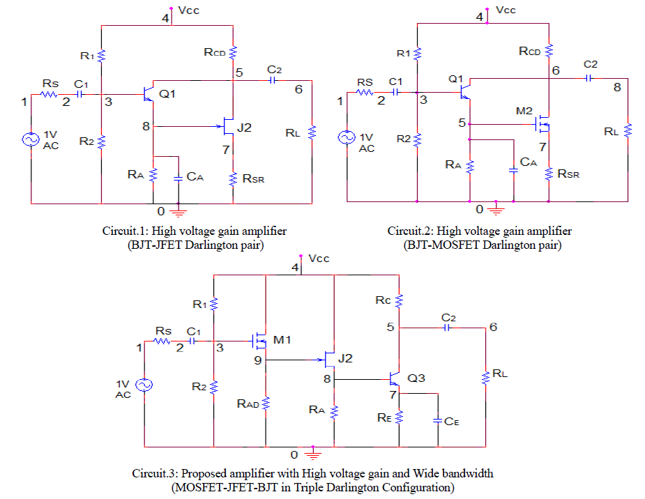
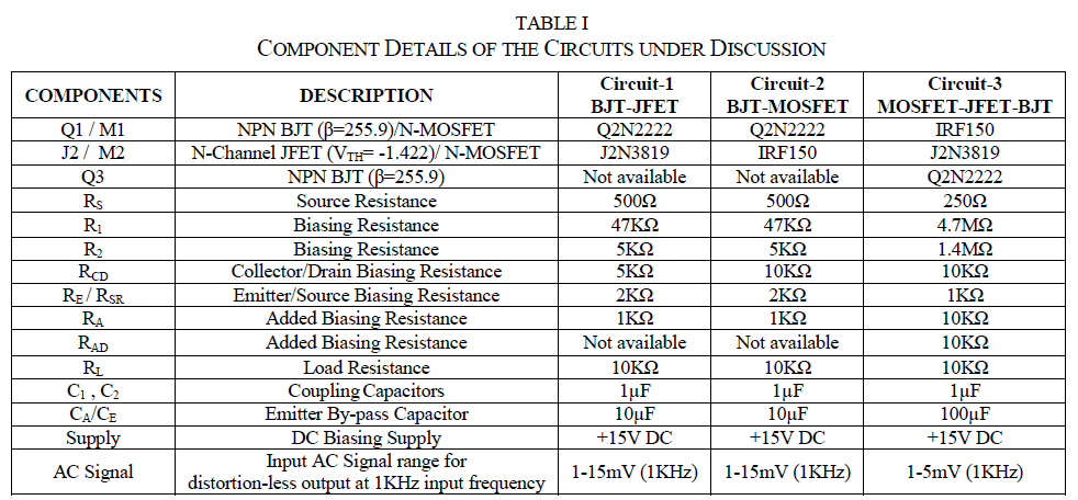
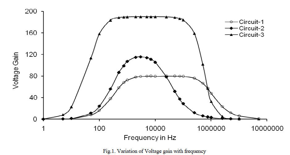
| Present investigation starts with two differently configured small-signal amplifier circuits which are respectively consisting compound units of BJT-FET and BJT-MOSFET in Darlington pair [8], [12]. These circuits are depicted herein as Circuit-1 and Circuit-2 respectively and are treated as reference amplifiers for comparing with the qualitative performance of proposed amplifier. However, the proposed amplifier as depicted in form of Circuit-3, is obtained by using a compound assembly of |
| MOSFET, FET and BJT in Triple Darlington configuration [11]. Unlike reference amplifiers, the drain points M1 and J2 in proposed amplifier are directly connected to the biasing supply VCC. In addition, two additional biasing resistances RA and RAD are incorporated in the proposed amplifier (Circuit-3) along with the bypass capacitor across emitter resistance. All the three amplifier circuits are properly biased using potential divider network with biasing parameters as described in Table I. |
| The amplifiers under discussion are biased with +15V DC power supply. Respective observations are made by feeding the amplifier circuits with 1V AC input signal source from which, a small and distortion less AC signal of 1mV for all the three amplifiers at 1KHz frequency is drawn as input for the amplification purpose. All the observations mentioned in the present manuscript are furnished through PSpice simulation software [3]-[5], [7], [9]-[13] (Student version 9.2). |
 |
 |
III. OBSERVATIONS AND DISCUSSIONS |
| Amplifiers of Circuit-1 and Circuit-2 provide fair and distortion-less results in 1-15mV range of AC input signals whereas for proposed amplifier of Circuit-3, it is received in 1-5mV range. However, the performance of the amplifiers are observed and discussed at 1mV, 1 KHz AC input signal. |
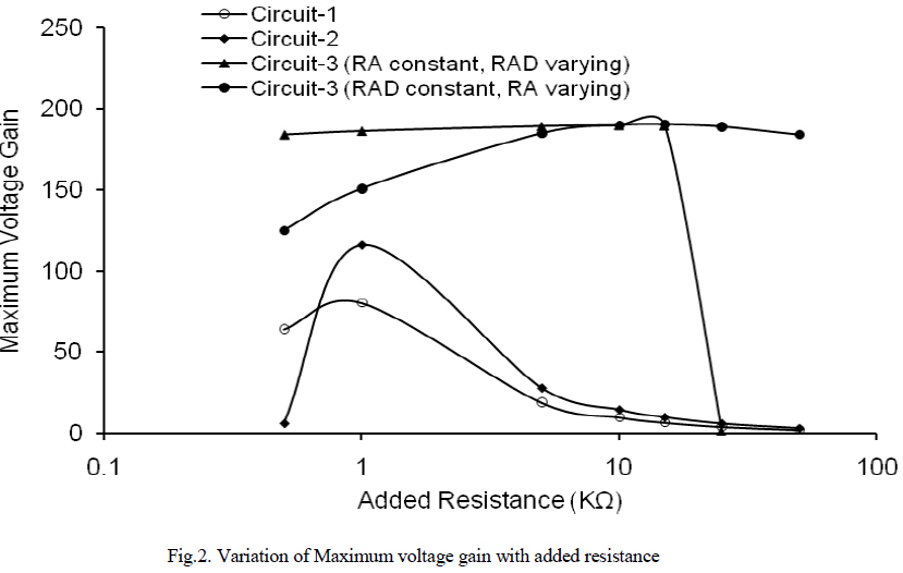
| Variation of maximum voltage gain as a function of frequency for all the three amplifiers are depicted in Fig.1. It is found that the amplifier of Circuit-1 produces 79.965 maximum voltage gain, 23.925 maximum current gain, 749.391KHz bandwidth (with lower cut-off frequency fL=475.459Hz and upper cut-off frequency fH=749.867KHz), 7.213μA peak output current and 72.132mV peak output voltage. However, amplifier of Circuit-2 produces 115.522 maximum voltage gain, 35.242 maximum current gain, 22.258KHz bandwidth (with fL=443.567Hz and fH=22.702KHz), 10.661μA peak output current and 106.607mV peak output voltage and the proposed amplifier of Circuit-3 produces 189.846 maximum voltage gain, 16.542K maximum current gain, 369.529KHz bandwidth (with fL=66.315Hz and fH=369.596KHz), 19.279μA peak output current and 192.786mV peak output voltage. Hence, it is clear that the bandwidth of proposed amplifier lies approximately midway of the bandwidth values of two reference amplifiers whereas maximum voltage and current gains are found to be considerably higher than both of them. |
 |
| In fact polarity of the composite unit of Darlington pair is determined by the driver device [14]. For example, a composite unit consisting BJT driver and JFET output (as in Circuit-1) will principally behaves like a BJT dominating Darlington unit. This is why the overall property of composite unit of the proposed amplifier seems to be inclined more towards MOSFET and motivates respective circuit to produce extra ordinarily high current gain. However, significantly high voltage gain of the proposed amplifier is perhaps due to the presence of complex combination of three dissimilar active devices and two additional biasing resistances in the circuit configuration. |
| It is to be noted that every amplifier under discussion shows phase reversal in respective output waveforms [5], [7]-[8], [12]. In fact, Common Emitter BJTs, Common Source FETs and Common Source MOSFETs independently produce phase reversal in their respective output waveforms [1]-[2], [8], [12]. This phase switching property of independent active devices is responsible to produce 180o phase difference in the output waveform of reference and proposed amplifiers which are using composite unit of BJT-JFET, BJT-MOSFET and MOSFET-JFET-BJT in their respective circuit configurations [2]-[3], [5], [7], [10]. |
| Maximum voltage gain of all the three amplifiers under discussion significantly depends on the added resistances. Dependency of maximum voltage gain on added resistances RA or RAD is graphically depicted in Fig.2. For reference amplifiers (Circuit-1 and Circuit-2) voltage gain found its maximum at RA=1KΩ and thereafter decreases almost exponentially at higher values of RA. However for amplifier of Circuit-3, when RA is constant and RAD is varying, the maximum voltage gain shows a non-linear increase up to 10 KΩ, and then falls abruptly to its lowest value at 25KΩ. On the other hand, when RAD is constant and RA is varying, voltage gain gradually increases to its maximum at 15 KΩ, and then starts decreasing with a slow pace. |
| Variation of maximum voltage gain with Source/Emitter resistance is shown in Fig.3. For reference amplifier of Circuit-1, the maximum voltage gain increases up to 2KΩ value of RE then tends toward sustained level. It indicates that this reference amplifier provides optimum performance for RE≥2KΩ. However, the increasing values of source resistance RSR for reference amplifier of Circuit-2 do not affect the voltage gain. It is also noticed here that if source resistance of this reference amplifier (Circuit-2) is removed, maximum voltage gain, maximum current gain and THD of the circuit rises fractionally and reaches to 115.872, 35.288 and 3.50% respectively while its bandwidth reduces to 21.458 KHz (with fL=449.388Hz and fH=21.908KHz). Conclusively, removal of RSR from the Circuit-2 hardly affects the performance of amplifier. |
 |
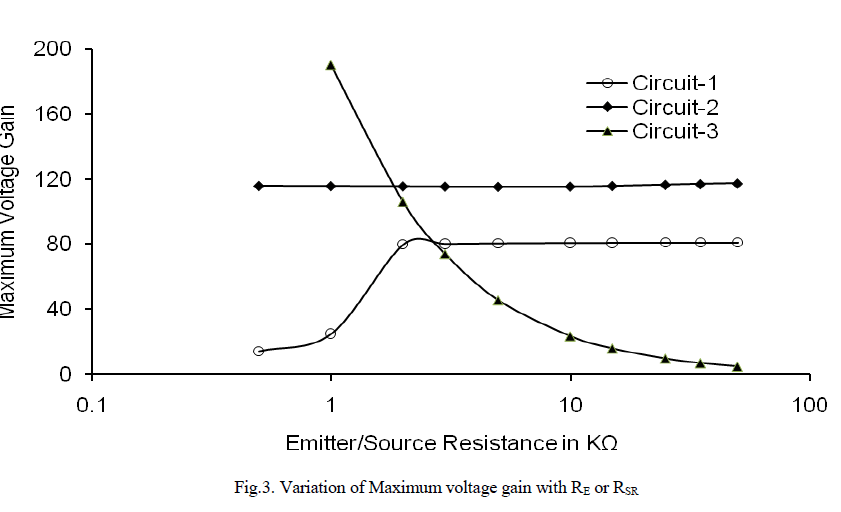 |
| Simultaneously, at increasing values of emitter resistance, the maximum voltage gain of the proposed amplifier (Circuit-3) decreases almost exponentially from 189.846 (at 1KΩ) to 4.893 (at 50KΩ). Since the resistance RE in the proposed amplifier circuit virtually behaves as source resistance for MOS driven composite unit therefore the source degeneration property of common source MOSFET amplifier forces voltage gain to fall almost exponentially with RE (Fig.3). More or less the similar situation persists for additional biasing resistance RAD which causes maximum voltage gain to fall rapidly after a critical limit of 25KΩ (Fig.2). |
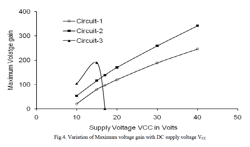 |
| Variation of maximum voltage gain with DC supply voltage VCC is depicted in Fig.4. Figure suggests that voltage gain of all the amplifiers under discussion rises nonlinearly at increasing values of VCC but that for proposed amplifier it drops to a lowest point at VCC=17V. It is also observed that the permissible range of supply voltage for reference amplifiers (Circuit-1 and Circuit-2) is 10-40V while for proposed amplifier of Circuit-3, this range is substantially reduced to 10-17V. This is perhaps due to MOSFET driven Triple Darlington unit of the proposed amplifier which bears a threshold voltage of 2.831V along with a high driving voltage at node 3. This driving voltage (at node 3) increases with VCC and reaches to 3.90V at 17V of VCC. This simply means that the MOSFET conducts for a driving voltage range of 2.831-3.90V corresponding to 10-17 volts of VCC. As VCC increases beyond 17V, the channel width broadens and causes sudden enhancement in ID. This in turn forces for an abrupt voltage drop across the load and distorts the frequency response curve. |
| During the course of qualitative analysis, authors attempted to study the performance of proposed amplifier (Circuit-3) by imposing some changes in the circuit configuration. Respective observations are listed below- |
| 1. When the added resistance RA is removed from the proposed amplifier (Circuit-3) opposite half cycles of the output voltage/current waveforms do not remain identical. Instead, the negative half cycle gets slightly suppressed and widen but the periodicity of positive and negative half cycles is retained and THD of the circuit increases in multifold. However, when the added resistance RAD is removed from proposed amplifier (Circuit-3), the maximum voltage gain reaches below unity, THD increases to a little and the output waveform bears only 43.55o phase difference instead of usual state of phase reversal. |
| 2. It is also observed that when drain point of the MOSFET in proposed amplifier (Circuit-3) is detached from VCC (node- 4) and connected to node-5, the voltage gain falls to 169.421, bandwidth to 3.782KHz and current gain to 2.61K whereas THD increases to 2.01%. However when drain point of the JFET in proposed amplifier (Circuit-3) is detached from VCC (node-4) and connected to node-5, the voltage gain falls below unity to a value 0.235. On the other hand if drain point of the MOSFET and JFET in proposed amplifier (Circuit-3) are simultaneously detached from VCC and connected to node-5, the amplifier provides poor response at lower frequencies. |
| 3. Similarly, when biasing resistance R1 is removed from the proposed amplifier (Circuit-3), voltage gain falls to 121.076, bandwidth to 364.797KHz, current gain to 128.997 but THD increases heavily. |
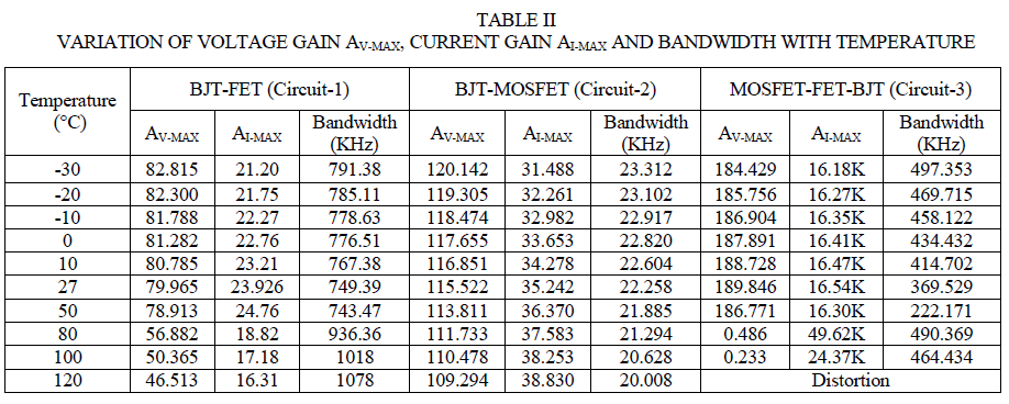
| Variation of voltage gain, current gain and bandwidth with temperature is also measured and listed in Table II. Table indicates that voltage gain of reference amplifier of Circuit-1 gradually decreases at increasing temperature. However, current gain increases but bandwidth decreases to a critical point of temperature (50°C) and thereafter the obtained nature reverse itself. For reference amplifier of Circuit-2, voltage gain and bandwidth gradually decreases whereas current gain increases throughout the rising temperature. On the other hand, for proposed amplifier (Circuit-3), voltage gain increases up to a critical limit of 27°C and then it reverses its nature. Similarly current gain also increases up to the critical limit (27°C) but decreases on 50°C, then again increases on 80°C and finally decreases on 100°C. However bandwidth decreases up to a critical limit of 50°C, then increases at 80°C and finally decreases at 100°C. |
 |
| Variation of maximum voltage gain with load resistance RL is also studied for all the three amplifiers under discussion (but not shown in form of graphs). It is observed that the voltage gain gradually rises up to 100KΩ value of RL for all the three amplifiers and then tends toward a saturation tendency at higher RL. This rising and saturation of the voltage gain with RL is found well in accordance of the usual behaviour of small signal amplifiers [2], [4], [5], [7], [12]. |
| Total Harmonic Distortion (THD) percentage for all the amplifiers under discussion is also calculated for 8 significant harmonic terms using established rules [12], [15]. It is found that the amplifiers of Circuit-1 and Circuit-2 show 3.75% and 3.48% THDs respectively whereas the proposed amplifier (Circuit-3) shows only 0.71% THD. In fact, MOS driven composite unit of the proposed amplifier virtually acquires the property of a MOSFET. The fast switching property of this virtually behaved MOS composite unit perhaps reduces the propogation delay between positive and negative half cycles of the output waveform. This decreases the distortion in output waveform and causes THD of the proposed amplifier to reduce to a significant limit |
IV. CONCLUSIONS |
| As a novel approach, three dissimilar active devices namely MOSFET, JFET and BJT are used in Triple Darlington configuration to explore a small-signal amplifier using RC coupling. This amplifier can effectively process small-signals ranging below 5mV at 1KHz in the frequency band of 66.315Hz to 369.596KHz. |
| The proposed small-signal audio amplifier (Circuit-3) is free from the problem of poor response of conventional small-signal Darlington pair or Triple Darlington amplifiers at higher order frequencies in the permissible frequency band. |
| With a moderate range bandwidth, proposed amplifier generates only 0.71% harmonic distortion and simultaneously produces high voltage and current gains of considerable value. High voltage as well as current gain logically sets its power gain greater than unity. All these features together make this amplifier fabulously unique in its class. |
| The proposed amplifier shows a considerable response in 0.5KΩ - 15KΩ range of additional biasing resistances RAD and RA . Its optimum performance is received for 10-17V DC supply voltage and voltage gain is observed maximum for 1KΩ value of emitter resistance RE |
ACKNOWLEDGEMENT |
| Authors gratefully acknowledge the facilities provided by the Department of Physics and Electronics, Dr. Ram Manohar Lohia Avadh University, Faizabad, U.P., India for the present investigations. Authors would also like to thank to other workers of the research group for their valuable suggestions and support during the development of present manuscript. |
References |
|