International Journal of Advanced Research in Electrical, Electronics and Instrumentation Engineering
ISSN ONLINE(2278-8875) PRINT (2320-3765)
ISSN ONLINE(2278-8875) PRINT (2320-3765)
K.Vinoth kumar1, R.Azhagumurugan2
|
| Related article at Pubmed, Scholar Google |
Visit for more related articles at International Journal of Advanced Research in Electrical, Electronics and Instrumentation Engineering
This project proposes the use of Switched boost inverter (SBI) which is a single-stage power converter derived from Inverse Watkins Johnson topology. Unlike the traditional buck-type voltage source inverter (VSI), the SBI can produce an ac output voltage that is either greater or less than the available dc input voltage. Also, the SBI exhibits better electromagnetic interference noise immunity when compared to the VSI, which enables compact design of the power converter. Another advantage of SBI is that it can supply both dc and ac loads simultaneously from a single dc input. These features make the SBI suitable for dc grid applications. In this paper, the SBI is proposed as a power electronic interface in dc grid. The structure and advantages of the proposed SBI-based grid are discussed in detail. This paper also presents a Genetic algorithm based PWM module, which reduces the harmonics in the output voltage. This paper also presents an overview of dq synchronous referenceframe- based controller for SBI, which regulates both dc and ac bus voltages of the nanogrid to their respective reference values under steady state as well as under dynamic load variation in the grid. Index Terms—Switched boost inverter, GA based PWM.
Keywords |
| Switched boost inverter, GA based PWM. |
INTRODUCTION |
| SBI is a single-stage power converter derived from Inverse Watkins Johnson (IWJ) Topology. This topology exhibits properties similar to that of a Z-source inverter (ZSI) with lower number of passive components and more active components. The SBI is a single input, two-output (one dc output and one ac output) power converter derived from IWJ converter and a VSI. Similar to the traditional twostage dc-to-ac conversion system, the SBI can also generate an ac output voltage that is either greater or less than the input dc voltage. However, the SBI has certain advantages when compared to the two stage conversion system shown which are discussed below: 1) Dead-Time Requirement: A shoot-through event in the inverter bridge of the two-stage conversion system damages the power converter stage, as well as the dc loads connected to the dc bus of the grid. So a dead-time circuit is necessary to minimize the occurrence of shoot-through events in this system. 2) Reliability and EMI Noise Immunity: Even with a dead time circuit, the probability of a shoot-through event cannot be eliminated completely because an EMI noise can also cause shootthrough in the inverter phase legs. With the use of SBI, the shoot-through event does not damage the switches of the power converter. So, SBI exhibits better EMI noise immunity and hence has better reliability compared to the two-stage conversion system. |
 |
II. FEATURES OF SWITCHED BOOST INVERTER |
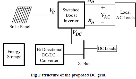
| Fig 1 shows the SBI based DC grid. SBI is a singlestage power converter that can supply both DC and AC loads (between nodes simultaneously from a single dc input. So, it can realize both the DC to DC converter for solar panel and the DC-to-AC converter in a single stage. This decreases size and cost of overall system. |
| The output ac voltage of SBI can be either higher or lower than the available source voltage. So, it has wide range of obtainable output voltage for a given source voltage. SBI exhibits better electromagnetic interference (EMI) noise immunity when compared to a traditional voltage source inverter (VSI), as the shoot-through (both switches in one leg of the inverter bridge are turned ON simultaneously) due to EMI noise will not damage the inverter switches. This reduces extra burden on the power converter protection circuit and helps in realization of compact design of the power converter. |
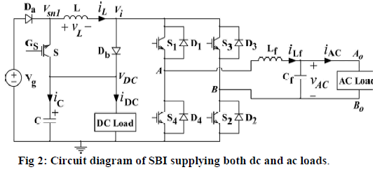
| As the SBI allows shoot-through in the inverter legs, it does not require a dead-time circuit and hence eliminates the need for complex dead-time compensation technologies This project presents a structure of the SBI-based dc grid and its advantages compared to the conventional structure This paper also describes the steady-state and small signal analysis of SBI supplying both dc and ac loads along with its PWM control technique.fig 2 shows the circuit of SBI configuration. |
 |
III. PWM CONTROL OF SBI |
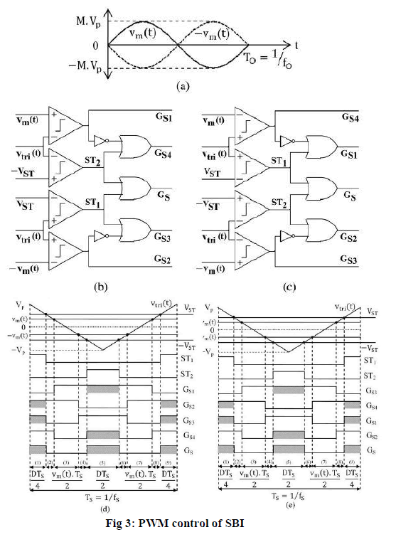
| The SBI utilizes the shoot-through interval of the Hbridge to invoke the boost operation. So, the traditional PWM techniques of VSI have to be modified to incorporate the shoot-through state, so that they are suitable for SBI. In a PWM scheme for SBI is developed based on the traditional sine-triangle PWM with unipolar voltage switching This technique has been illustrated in Fig.3 during positive and negative half cycles of the sinusoidal modulation signal vm(t) [shown in Fig. 3.(a). As shown in Fig. 3.(b) and (d), during positive half cycle of vm(t) (vm(t) > 0), the gate control signals GS 1 and GS 2 are generated by comparing the sinusoidal modulation signals vm(t), and –vm(t) [shown in Fig. 3.(a) with a high-frequency triangular carrier vtri(t) of amplitude Vp . The frequency fS of the carrier signal is chosen such that fS _fO . Therefore, vm(t) is assumed to be nearly constant in Fig. 3.(d). The signals ST1 and ST2 are generated by comparing vtri(t) with two constant voltages VST and –VST, respectively. The purpose of these two signals is to insert the required shootthrough interval D·TS in the PWM signals of the inverter bridge. Now the gate control signals for switches S3 , S4 , and S can be obtained using the logical expressions given as follows: GS3 =GS2+ST1 ; GS4 =GS1 +ST2 ; GS = ST1 +ST2 . |
 |
COMPARISON OF SBI WITH A TRADITIONAL TWO-STAGE DC-TO-AC CONVERSION SYSTEM |
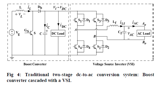 |
| In the previous section, it is shown that the SBI is a single input, two-output (one dc output and one ac output) power converter derived from IWJ converter and a VSI. Similar to the traditional two-stage dc-to-ac conversion system shown in Fig. 4, the SBI can also generate an ac output voltage that is either greater or less than the input dc voltage. However, the SBI has certain advantages and limitations when compared to the two stage conversion system shown in Fig. 4, which are discussed below: |
| 1) Extreme Duty Cycle Operation: At the extreme duty ratio operation (e.g., for D ≥ 0.75) of a conventional boost converter, the inductor L is charged over a longer time duration in the switching cycle, and very small time interval is left to discharge the inductor through the output diode Db . So this diode should sustain a short pulse width current with relatively high amplitude. Also, this causes severe diode reverse recovery current and increases the EMI noise levels in the converter. This also imposes a limit on the switching frequency of the boost converter and thus increases the size of the passive components used in the two-stage conversion system. In case of SBI, the maximum shoot-through duty ratio is always limited to 0.5 for a positive dc bus voltage VDC. So, even when the converter operates at the point of maximum conversion ratio, the conduction time of the diodes Da , Db of SBI is approximately equal to 50% of the switching time period, which alleviates the problems due to extreme duty ratio operation of a boost converter. So, SBI can operate at relatively higher switching frequencies compared to the traditional two stage conversion system. This also decreases the size of passive components used in the power converter. |
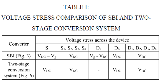 |
| 2) Voltage Stress of Switching Devices: Table I compares the voltage stress of the semiconductor devices used in the SBI and the two-stage conversion system shown in Fig. 6. From this table, it can be observed that the switch “S” has less voltage stress (VDC – Vg) in case of SBI. For all other devices, the voltage stress is same for both SBI and the two-stage conversion system. |
| 3) Maximum Conversion Ratio: The maximum conversion ratio (VDC/Vg ) of a practical boost converter cannot exceed 3.0 (approximately), due to the effects of various non-idealities such as DCR/ESR of the passive components, on-state voltage drops of the semiconductor devices, etc. This value may slightly vary depending on the actual values of non-ideal elements present in the converter. Similarly, the rms AC output voltage (VAC (rms)) of a single-phase inverter using sinusoidal PWM cannot exceed 1/√2 times the dc link voltage (vDC) in the The rms ac-to-dc conversion ratio of the two-stage conversion ratio may be increased slightly by using semiconductor devices with very low forward voltage drops and passive components with very low ESR/DCR. This enhances the overall cost of the power converter stage. Another way to increase the conversion ratio of the two-stage conversion system is to use high step-up dc-to-dc converters or the converters with transformer/ coupled inductor. These converters require additional semiconductor devices and passive components which increase the size as well as cost of the power converter stage. In this paper, it is shown experimentally in Section V that the maximum rms ac-to-dc conversion ratio of the SBI is 2, which is comparable to that of a two-stage conversion system. |
| 4) Number of Control Variables: Similar to a twostage conversion system, the SBI also has two control variables: Shoot through duty ratio (D) and the modulation index (M).The DC busVoltage (vDC) is controlled by D, while ac output voltage of the converter is controlled by M. However, similar to ZSI, the value one of these two control variables decides the upper limit of the second control variable of SBI. The mathematical relation between D and M depends on the control technique used. Note that, as mentioned above, it is possible to extend most of the PWM control techniques of ZSI to control the SBI. |
| 5) Number of Devices: As shown in Fig.3, the SBI requires five active switches, six diodes, two inductors, and two capacitors for its realization. The two-stage conversion system shown in Fig. 6 uses only one diode (Da ) less compared to the SBI. However, in a DC grid, the input comes from a renewable energy source, e.g., solar panel or fuel cell, which should always be associated with a series diode to block the reverse power flow. So the diode Da of SBI can be a part of the renewable energy source which eliminates the need for an external diode. Thus, the number of devices in both converters is same. |
IV. IMPLEMENTATION OF GENETIC ALGORITHM |
| The idea of evolutionary computing was introduced in 1960 by I.Richenberg. Genetic algorithms are computerized search and optimization algorithms based on the mechanics of natural genetics and natural selection. Genetic algorithms are good at taking large search spaces and navigating them looking for the optimal solution. A more striking difference between genetic algorithms and other traditional optimization methods is that, genetic algorithm uses a population of points at one time in contrast to single point approach by traditional methods. |
Roulette-Wheel Selection |
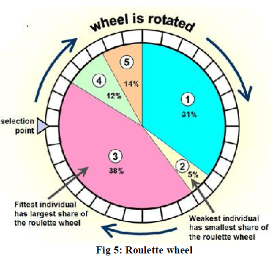
| Roulette wheel selects the best chromosome in the population by rotating a roulette-wheel, whose circumference is marked proportional to the stringâÃâ¬ÃŸs fitness value. Thus ith string in the population is selected with a probability proportional to (Fi). Where (Fi) is the fitness value for that string. As the population size in a simple GA is kept fixed, the sum of probabilities of selecting each string should be 1. Thus the individual string with a higher fitness value is expected to be selected by the Roulettewheel pointer as shown in Fig 5. |
 |
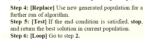
STEPS INVOLVED IN GENETIC ALGORITHM |
 |
 |
Flow chart: |
 |
SIMULATION OF SWITCHED BOOST CONVERTER |
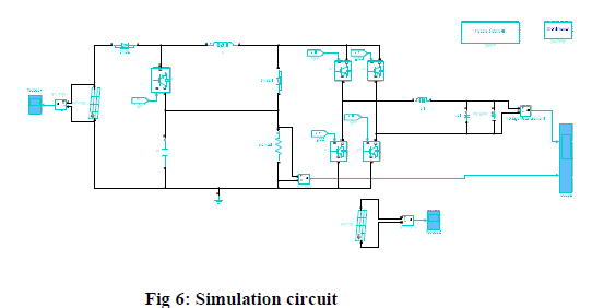 |
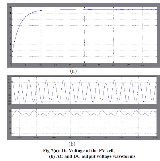
| As shown in fig 6 an open- loop simulation of the proposed model is performed using MATlab simulink.genetic algorithm based pulse width modulation is used to reduce the harmonics and improve the efficiency.The simulation results are shown in fig 7a. the input dc voltage from the PV cell and the AC and DC load voltages are shown in fig 7b. respectively.The output voltage is boosted as compared with the input DC,with the help of the switched boost configuration. |
V. SIMULATION RESULTS |
 |
VI. CONCLUSION |
| This paper has provided a brief summary of This project presents a novel power electronic interface called switched boost inverter (SBI) for DC grid applications. It is shown that the SBI is a single-stage power converter that can supply both dc and ac loads simultaneously from a single dc input. It is also proven that the SBI can generate an ac output voltage that is either higher or lower than the available source voltage. This project also describes the advantages and limitations of SBI when compared to the ZSI and the traditional two-stage dc-to-ac conversion system. The steady-state and small-signal analysis of the SBI supplying both dc and ac loads, and a PWM control technique suitable for SBI are also described in this project |
References |
|