International Journal of Advanced Research in Electrical, Electronics and Instrumentation Engineering
ISSN ONLINE(2278-8875) PRINT (2320-3765)
ISSN ONLINE(2278-8875) PRINT (2320-3765)
| Nandisha. Y PG student [DCE], Dept. of TCE, Siddaganga Institute of Technology, Tumkur, Karnataka, India |
| Related article at Pubmed, Scholar Google |
Visit for more related articles at International Journal of Advanced Research in Electrical, Electronics and Instrumentation Engineering
Synthetic Aperture Radar (SAR) is a well known technique for imaging the earth’s surface. This paper presents a wideband variable gain amplifier (VGA) which can be used in the direct conversion receiver (DCR) for SAR. This paper first introduces how to extract the important parameters i.e. gain, bandwidth and power consumption of the VGA from the overall receiver requirements. VGA has designed for 2.4GHz Bandwidth and simulations are done using 0.13um technology level-54 model files on HSPICE Simulator. The proposed VGA circuit has a variable gain of (4.43 – 15.14) dB and -3dB frequency falls at 2.398GHz. The power consumption is only 1.803mW and the supply voltage is about 1.8v.
Keywords |
| CMOS,Wideband, variable gain amplifier, low power consumption, differential amplifier. |
INTRODUCTION |
| Synthetic Aperture Radar (SAR) is a well known technique for imaging the earth’s surface. Some of its most important applications include disaster management, land and sea traffic observation, wide area surveillance, and environmental monitoring. SAR systems use radar signals and complex electronics to provide broad-area imaging capability. The most attractive feature of SAR systems is their ability to provide day-and-night imagery of earth, independent of weather conditions [1]. In order to overcome the limitation of imaging wide swath, with simultaneously high resolution, SAR systems employ receiving antenna with multiple sub-apertures, each sub aperture with its own independent receiver [2]. Each of the N sub apertures on the receive antenna has its own receiver. The digitized signals from each of these receivers can then be stored and digitallyprocessed a posterioris to form a high resolution image of a large area. In such a system it would be beneficial to realize each of the independent receivers with highly integrated CMOS circuits that have small silicon footprint andoverall low power consumption. The direct conversion receiver (DCR) which down converts the RF signal directly to its base band. DCR has the advantage that it requires no off-chip image reject filters. Moreover, it only requires low-pass filters and amplifiers that are amenable to monolithic integration. In this journal, the design of a wideband variable gain amplifier (VGA) is described which is to be used in the DCR for SAR systems. Therefore small silicon area and low power consumption are the basic goals for the design. |
LETERATURE SURVEY |
| FilipTavernier and MichielSteyaert,proposed “A low power limiting amplifier with area efficientoffset compensation in 90nm CMOS”. The largetime constant needed in the offset compensation feedback loop isboosted by an inverting amplifier to reduce the chip area [3]. On topof this, to reduce the chip area even more, negative capacitors areapplied to increase the bandwidth instead of making use of theinductive peaking technique. The proposed circuit has a smallsignalgain of 35dB and a bandwidth of 4.15GHz. The power consumption is having only 14.7mW. |
| Ville Saari,MikkoKaltiokallio, SaskaLindfors,JussiRyynänenandKari A.I.Halonen,proposed“A 240-MHz Low-Pass Filter With Variable Gain in65-nm CMOS for a UWB Radio Receiver” An integrated fifth-order continuous-time lowpassfilter for a WiMedia ultrawideband radio receiver is described inthis paper [6]. The passbandedge frequency of the implemented filter is 240 MHz in order toreceive multiband-orthogonal-frequency-division-multiplexingsignals using the direct-conversion topology. The voltage gain ofthe filter can be controlled from 9 to 43 dB in the 1-dB gain steps. The circuit uses a 1.2V supply. |
| YuanjinZheng, Jiangnan Yan, and Yong Ping Xu, proposed “A CMOS VGA With DC Offset Cancellation forDirect- Conversion Receivers”A CMOS dB-linear variable gain amplifier (VGA)with a novel I/Q tuning loop for dc-offset cancellation is presented.The CMOS dB-linear VGA provides a variable gain of 60 dB whilemaintaining its 3-dB bandwidth greater than 2.5MHz. A novelexponential circuit is proposed to obtain the dB-linear gain controlcharacteristics. Nonideal effects on dB linearity are analyzed andthe methods for improvement are suggested. A varying-bandwidthLPF is employed to achieve fast settling. The chip is fabricated in a 0.35μm CMOS technology. |
| Quoc-Hoang Duong, Chang-Wan Kim, and Sang-Gug Lee,proposed”A 95-dB Linear Low-Power Variable Gain Amplifier” this paper [8], designs the variable gain amplifier in 180nm CMOS technology uses the supply voltage of 1.8v and the variable gain of (47.5 - 95)dB. The -3dB frequency of 32MHz and having the power consumption is only 6.7mW. |
VARIABLE GAIN AMPLIFIER (VGA) |
A. STAGE-1 VGA: |
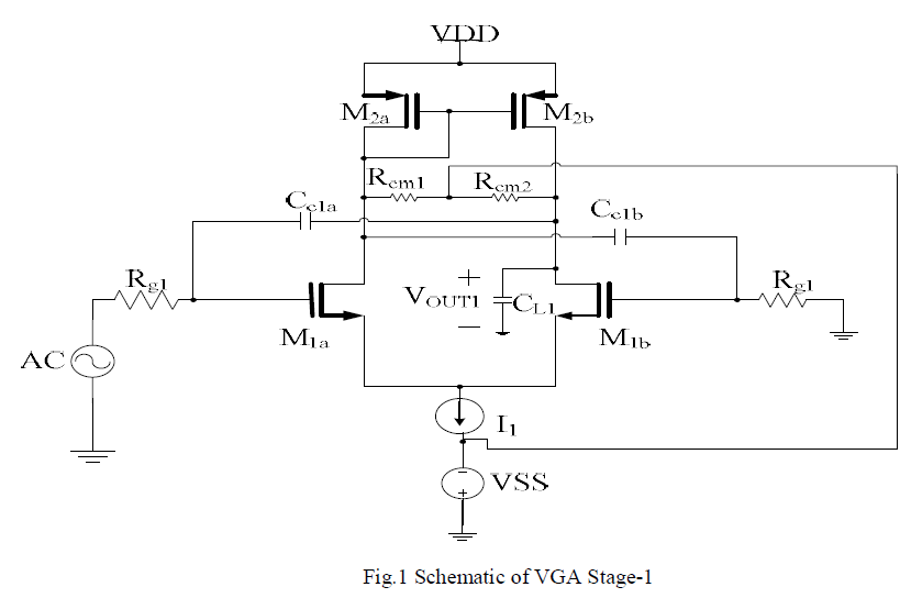
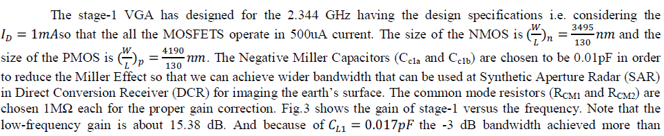
| The first stage of the VGA should be a high-gain, low-noise stage. Moreover the -3 dB bandwidth of this stage has to be much higher than the overall bandwidth of the VGA. Based on these requirements, a active loaded sourcecoupled differential pair was chosen. The schematic of the circuit is shown is Fig.1M1a and M1b form the sourcecoupled pair with active loads . The acts as a tail current source. Resistor Rg1 represents the resistance of the driving source. That the Miller effect increases the input capacitance and the pole formed by Rg1 and the total input capacitance of the stage limit the -3 dB bandwidth of the amplifier. In order to suppress the Miller-effect and increase the bandwidth of the stage, negative Miller capacitors (Cc1a and Cc1b) have been used. These capacitors were chosen to push the input pole to higher frequency. CL1 represents the capacitive loading at the output VOUT1. It includes the intrinsic capacitance of the transistor M1b, the wiring capacitance and the input capacitance of the next stage. |
 |
 |
 |
 |
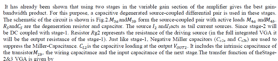
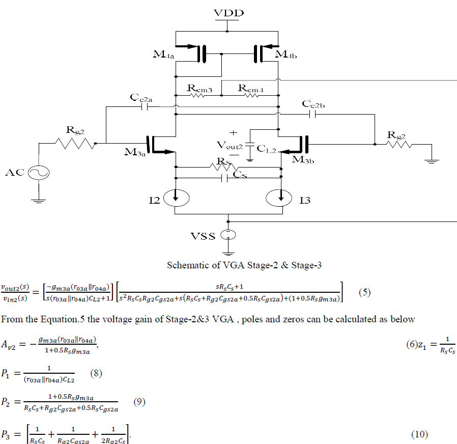
B. STAGE-2 & 3 VGA: |
 |
 |
SIMULATION RESULTS |
A. STAGE-1 VGA: |
 |
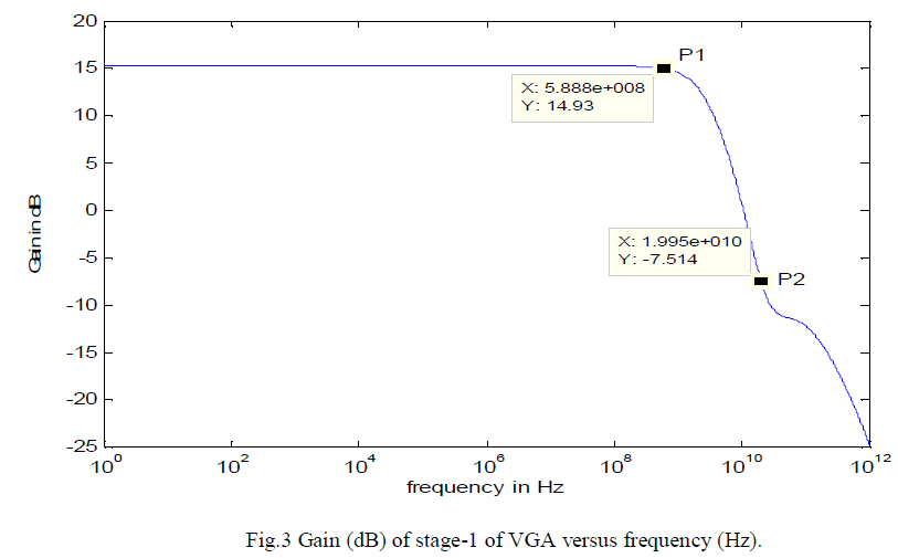
| 2.344GHz hence P1 becomes the dominant pole since CL1>Cg1sa . And power consumed in the circuit is 1.803mW. The Table.1 gives the performance comparison of present work with reference papers. |
 |
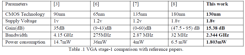 |
| From the Table.1we can conclude that designing of Stage-1VGA in 130nm CMOS Technology is better and good in terms of -3dB frequency is 2.344GHz and power consumption is only 1.803mW. The supply voltage required is 1.8v. |
B. VGA STAGE-2&3: |
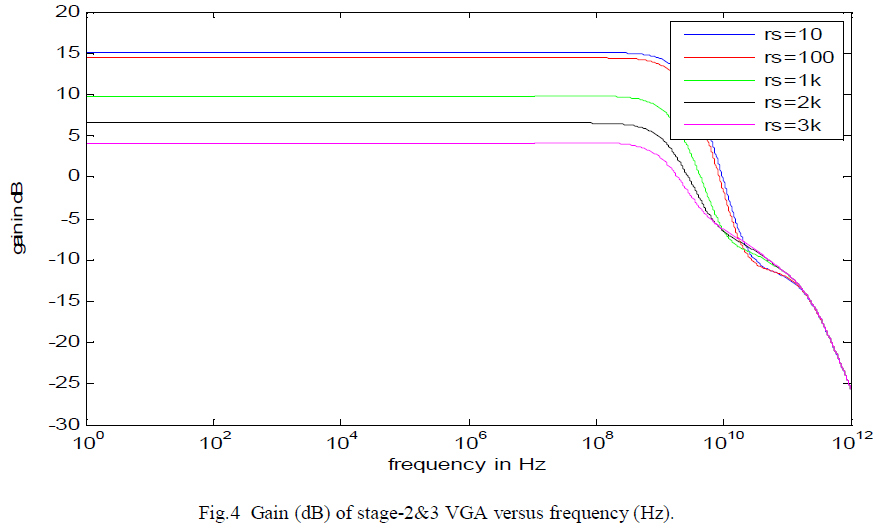
| The stage-2 & 3 VGA has designed for the 2.4 GHz having the design specifications i.e. considering the I1= 1mAand I3 = 1mA. The negative miller capacitors (Cc2a and Cc2b) are chosen to be 0.01pF in order to reduce the Miller Effect. The common mode resistors (RCM3 and RCM4) are chosen 1MΩ each for the proper gain correction. Fig.5.2.1 shows the gain of stage-2 & 3 versus the frequency. Note that the variable gain is about (4.43 - 15.14) dB. The -3 dB bandwidth of stage-2&3 is around 2.398GHz and the power consumed in the circuit is 1.832mW. The Table.2 gives the performance comparison of present work with reference papers. |
 |
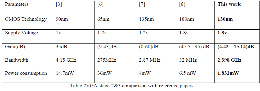 |
| From the Table.2, we can prove that the gain can be variable of (4.43 – 15.14)dB this can be achieved due to the different values of RS. The main focus of using RSin thedesign is to make variable the gain. The maximum bandwidth that we achieved is 2.398 GHz and the power consumed is only 1.832mW. |
CONCLUSION |
| This paper first explained the idea behind Synthetic Aperture Radar (SAR) since the VGA was to be used within such a system. Additional details about the receiver architecture for SAR were also provided. In the section- 2&3, the basic requirements such as Common-Source Amplifier and Differential Amplifier were needed to design VGA. Because of using Differential Amplifier with active load the Wider Bandwidth can be achieved as for the receiver design requirements. In the section-4.1 Stage-1 VGA has designed for 2.344 GHz bandwidth, 15.38dB of gain and power consumption was 1.803mW all these were presented which were extracted from the system requirements for the receiver. The section-4.2 presents variable gain of (4.43 – 15.14) dB, Bandwidth was 2.398 GHz and the power dissipation was 1.832mW. All these simulations were done using 0.13um technology level-54 model files on HSPICE Simulator. |
ACKNOWLEDGEMENT |
| Author would like to thank Dr. K C NarasimhaMurthy, Professor & Head, Dept. of TCE, Siddaganga Institute of Technology, Tumkur, for his support and suggestions in completing this journal paper. |
References |
|