


 29 / 34

Page 66
Notes:
conferenceseries
.com
RRJOMS | Volume 5 | Issue 4 | July, 2017
July 27-29, 2017 Vancouver, Canada
10
th
International Conference on
Emerging Materials and Nanotechnology
Photochromic organic field-effect transistors: Molecules, device properties and laser patterning of
circuits
Yutaka Wakayama
National Institute for Materials Science, Japan
W
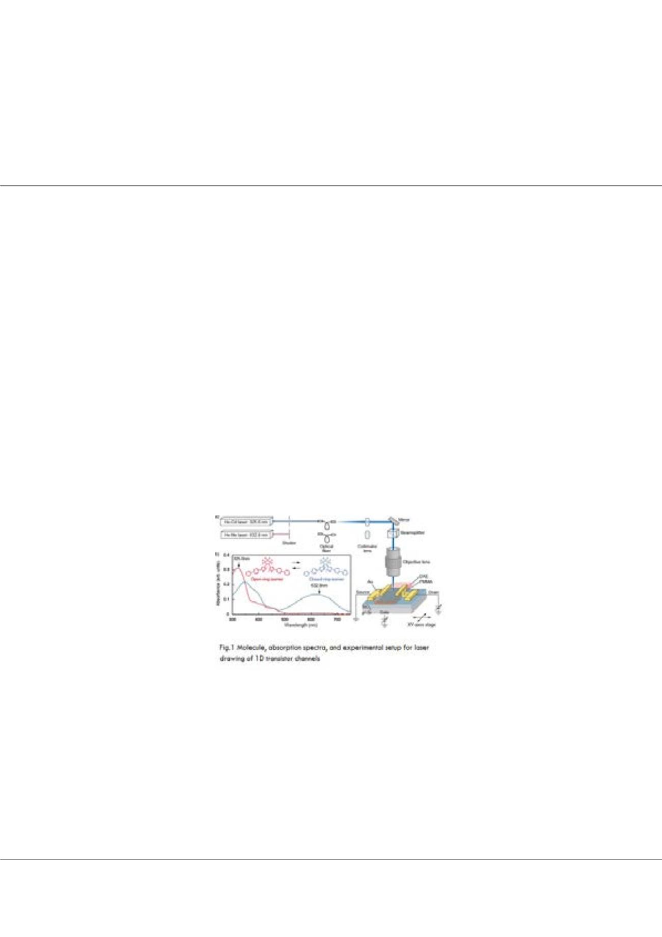
e developed an optically controllable organic field transistor (OFET) by employing photochromic diarylethene (DAE)
molecules as a transistor channel layer. DAE molecules are known to undergo photochromic reaction, i.e., reversible
conformational change between closed- and open-ring isomers by alternating ultraviolet (UV) and visible (VIS) light irradiation.
We found that the drain current in the DAE-based OFET also showed reversible change accompanied by this conformational
change; the closed-ring isomer produced by UV light exhibited a transistor operation under appropriate gate and drain bias
voltages, meanwhile the open-ring isomer produced by VIS light showed no drain current. As a result, a remarkably high on/off
ratio of 1,000 was achieved. The drain current modulation can be attributed to the drastic transformation in the π-conjugation
system in association with the photo-isomerization. These results present two important messages. The first one is that this
compound has dual properties: organic semiconductor and photochromism. The second is that a phase transition between
semiconductor and insulator can be induced by light irradiation. Based on these achievements, we demonstrate laser drawing
of one-dimensional (1D) channels on an OFET with a photochromic DAE layer. The main findings are: i) a number of 1D
channels can be written and erased repeatedly in the DAE layer by scanning UV and VIS focused laser spots alternately between
the source and drain electrodes, ii) the conductivity of the 1D channel can be controlled by the illumination conditions, and
iii) it is possible to draw an analogue adder circuit by optically writing 1D channels so as to overlap a portion of the channels
and perform optical summing operations by local laser illumination on the respective channels. These findings will open
new possibilities of various optically reconfigurable low-dimensional organic transistor circuits, which are not possible with
conventional thin film OFETs.
Biography
Yutaka Wakayama has served as a Research Engineer at Asahi Glass Company from 1989 to 1994. He was a research staff member at Tanaka Solid Junction
Project, ERATO, JST from 1994 to 1998 and received his PhD degree from University of Tsukuba in 1998. After working as a Post-doctoral fellow at Max-
Planck Institute for Microstructure Physics, Germany in 1998-1999, he has joined National Institute for Materials Science (NIMS) in 1999. At present, he belongs
to International Center for Materials Nanoarchitectonics (WPI-MANA) of NIMS. His current research interests are self- and directed-assemblies of molecules,
functional organic field-effect transistors and molecular nano-electronics.
WAKAYAMA.Yutaka@nims.go.jpYutaka Wakayama, Res. Rev. J Mat. Sci. 2017
DOI: 10.4172/2321-6212-C1-002