Keywords
|
| Multi-level inverter, SVPWM, redundant states, THD, Cascaded H-Bridge inverter SVPWM. |
INTRODUCTION
|
| The Multilevel inverters is promising power electronics topology for high power high voltage applications. Because of its low electromagnetic induction and high efficiency [1]. These inverters can solve the problem associated with traditional two level inverters. Their topologies including diode clamped , flying capacitor and cascaded H-bridge structures are intensely studied for high power applications .The cascaded inverters topology has several advantages that have made it attractive in power conditioning systems and medium and high power drive applications. The first advantage is ease of regulation of DC bus .The second advantage is modularity of control can be achieved unlike diode clamped and capacitor clamped inverters where individual phase legs must be modulated by central controller. Large number of states offered by multi level converters can impose massive computational overhead if not carefully optimized .Among all the switching algorithms [4- 6]space vector modulation seems most promising since it offers a great flexibility in optimizing switching pattern design and also well suited for digital implementation. The space vector modulation for more than three level inverter is very complex due to large number of space vectors and redundant switching states and calculation of dwell times is also complicated [5]. A simplified space vector algorithm is proposed in this paper where the location of reference voltage vectors and calculation of dwell times is simplified with minimum voltage harmonic content .For a particular reference voltage it is easy to determine all the redundant switching states and determine the status of switching states whether it is large, small or medium and automatically generates that pattern which need not require any look-up table, hence minimizing the memory requirement and complexity. And can be applied to high level cascaded H – bridge inverters. |
CASCADED H-BRIDGE INVERTER
|
| Cascaded H-bridge multilevel inverter has been used multiple units of H-bridge power cells connected in series to achieve medium voltage operation and low harmonic distortion. This inverter needs several DC sources to synthesize the output voltage waveform. The single H- Bridge can generate three-level output. When S11 and S21 are on, the output is +Vdci; when S31 and S41 are on, the output is −Vdci; when either pair S11 and S31 or S41 and S21 are on, the output is 0.In symmetric structure of cascaded H-bridge inverter which the DC voltage sources are equal, there are 2N+1 level in output of phase voltage where N is the number of DC voltage sources. The asymmetric input voltages when properly chosen eliminate redundant output levels and maximize the number of different levels generated by the inverter. Therefore with fewer number of semi conductor switches this topology can achieve the same output voltage quality.The number of levels in phase voltage obtains as |
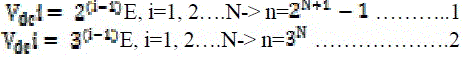 |
| Where N is the number of DC voltage sources |
| The optimal asymmetry has been obtained using voltage sources proportionally scaled to the two- or three- H-bridges. |
| The various switching states for nine level inverter with inverter H bridge voltages E and 3E are summarizedin Table1.It is worth noting that the inverter phase voltage VAN may not necessarily equal the load phase voltage VAC, which is the voltage at node A with respect to the load neutral O. It can be observed from Table1 that some voltage levels can be obtained by more than one switching state. |
SPACE VECTOR MODULATION
|
| The Cascaded H-Bridge uses multiple units of H-bridge sources connected in series to produce high AC output voltages. In the proposed algorithm space vector in α- β axis is decomposed in integer scale, which makes an angle of π/3, it is easy to find out coordinates of any space vectors. The location of the reference voltage vector and the dwell times of the space vectors can be calculated easily. For the 9-level inverter, there are 384 small triangles and the vertex of each triangle represents a space vector. The hexagonal vectors can be divided into six major triangular sectors (I to VI). Only the first sector of the coordinate is used because the vectors located in the other sectors can be transformed to first sector by clockwise rotating by an angle of K*pi/3 , k =(1,2,3,4,5 for sector 2 to 6). As all the sectors are identical, only details of sector1is given. Vertex of each triangle represented as space vector defined by |
 |
| Va, Vb and Vc are phase voltages of The co-ordinate of each vector in a Cartesian co-ordinate system Vx, Vy can be calculated as |
 |
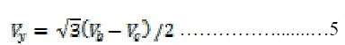 |
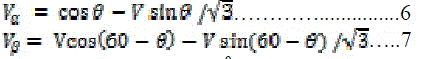
| The co-ordinates of space vector with unity DC supply voltage (Vdc = 1 p.u). To reduce voltage harmonic distortion, the reference voltage V* can be synthesized by nearest vector,Because of complexity involved in calculation of dwell lines and identification of triangle where the reference vector end point fall s Cartesian co-ordinate system can be transferred to 60° co-ordinate system. |
 |
| |
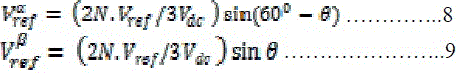
| Where Vα and Vβ are the co-ordinates of a space vector in 600 co-ordinate system V and are length (amplitude) and phase angle respectively. The reference vector after decomposition into α and β (600 in axis) For N+1 level inverter the component along α- β axis for reference vector can be written as |
 |
| Where θ is the speed of rotation. |
| Any reference vector Vref and θ lying in a rectangular area specified by ABCD. |
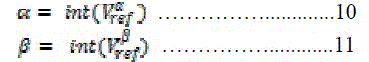
| However we can obtain rounded integer values (α, β) |
 |
| These α, β are defined by vector (α, β) in α- β axis |
 |
| The Vref is located in ABD, otherwise BDC If the corresponding three nearest space vectors are (α1, β1) and (α2, β2) and (α3, β3) then dwell times are calculated as |
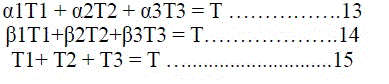 |
| Where T is PWM time period. |
 |
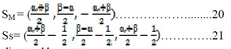 |
| Where SL, SM and SS are small, medium and large states. |
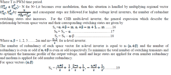
| The switching states in other sectors (II to VI) can be obtained as, |
| In multilevel inverter, the redundant states increase with the voltage level. For example seven and nine level inverters have .The redundant states of six and eight respectively for zero voltage vector. This redundancy is employed to minimize voltage harmonic distortion. The switching sequence design is selected to meet the requirements such as minimization of number of switching’s per sampling period and one voltage level change for commutation of switch and adoption of large small and medium states. The corresponding sequence design is given in Table-3 for the next half the sequences are employed from last to first. |
| For the next half the sequences are employed from last to first. |
RESULT AND DISCUSSION
|
| The simulation results corresponding to =0.8 for seven and nine level inverter are shown .The output voltage is compatible with load The Induction Motor Load is taken with rating of Load: 5HP, 400V, 50Hz, 1000rpm; Stator Resistance and Inductance: 0.01965 p. u. and 0.0397 p. u.; Rotor Resistance and Inductance: 0.0109 p. u. and 0.0397 p. u. with Mutual Inductance: 1.359 p. u., Sampling time Ts=10e-6 sec. This method features easy implementation and more importantly, minimum harmonic content in the inverter output voltage and current of the Induction Motor Load. For seven level output the current THD is 1.24% and the Line voltage THD is 9.32%where as . For nine level the current THD reduces, which is 0.66%and line voltage THD is 6.02%. As different voltages can be obtained by simply changing the modulation index . So, the results are shown as follows. |
| In Fig 3 , it shows the Simulink model of nine level asymmetric Cascaded H bridge inverter with input dc voltages as 100V and 300V corresponding to =0.8 with Induction Motor Load is taken with rating of Load: 5HP, 400V, 50Hz, 1000rpm |
| In Fig 4 , it shows the output line voltages of nine level Cascaded H bridge inverter corresponding to =0.8 with Induction Motor Load is taken with rating of Load: 5HP, 400V, 50Hz, 1000rpm |
| In Fig 5 , it shows the output line voltages THD of nine level Cascaded H bridge inverter corresponding to =0.8which is 6.96 with Induction Motor Load |
| In Fig 6 , it shows the output line currents of nine level Cascaded H bridge inverter corresponding to =0.8 withInduction Motor Load is taken with rating of Load: 5HP, 400V, 50Hz, 1000rpmthe current THD reduces, which is 0.66%. |
| In Fig 7 , it shows the output line voltages of seven level Cascaded H bridge inverter corresponding to =0.8 with Induction Motor Load is taken with rating of Load: 5HP, 400V, 50Hz, 1000rpm |
| In Fig 8 , it shows the output line voltages THD of seven level Cascaded H bridge inverter corresponding to =0.8which is 9.32 with Induction Motor Load |
| Fig .9 shows the Torque output of seven level Cascaded H bridge inverter. The Induction Motor Load is taken with rating of Load: 5HP, 400V, 50Hz, 1000rpm; Stator Resistance and Inductance: 0.01965 p. u. and 0.0397 p. u.; Rotor Resistance and Inductance: 0.0109 p. u. and 0.0397 p. u. with Mutual Inductance: 1.359 p. u., Sampling time Ts=10e-6 sec. |
| Fig .10 shows the Torque output of seven level Cascaded H bridge inverter. The Induction Motor Load is taken with rating of Load: 5HP, 400V, 50Hz, 1000rpm; Stator Resistance and Inductance: 0.01965 p. u. and 0.0397 p. u.; Rotor Resistance and Inductance: 0.0109 p. u. and 0.0397 p. u. with Mutual Inductance: 1.359 p. u., Sampling time Ts=10e-6 sec. |
CONCLUSION
|
| The proposed Space Vector Pulse Width Modulation method simplifies the calculation of space vectors and their corresponding dwell times to facilitate the design and digital implementation .All the space vectors are transformed to 60° co-ordinate system .This algorithm features automatic switching pattern generation with minimum harmonic content in the inverter output voltage and current of induction motor load. This algorithm is verified for five, seven, nine level cascaded H bridge inverter through MATLAB/SIMULINK simulations. |
ACKNOWLEDGEMENT
|
| We thank the University Grants Commission (UGC), New Delhi for providing Major Research Project to carry out the research in the area of Multi level inverters. |
Tables at a glance
|
|
|
| |
Figures at a glance
|
 |
 |
 |
 |
| Figure 1 |
Figure 2 |
Figure 3 |
Figure 4 |
 |
 |
 |
 |
| Figure 5 |
Figure 6 |
Figure 7 |
Figure 8 |
 |
 |
 |
| Figure 9 |
Figure 10 |
Figure 11 |
|
| |
References
|
- J. Rodríguez, J. Lai, and F. Peng, “Multilevelconverters: a survey of topologies, controls andapplications,” IEEE Trans. Ind. Electron., Vol. 49,No.4, pp. 724-738, Aug. 2002
- Sanmin Wei and Bin Wu “A General Space Vector PWM control Algorithm for Multi-level inverters” IEEE 2003, pp 562-568
- j. s. lai and f. z. peng, “multilevel converters – a new breed of power converters,” ieee trans. ind. appl., vol.32, no.3, pp. 509-517, may/jun.1996.
- l. yiqiao, and c.o. nwankpa, “a new type of statcom based on cascading voltage source inverters with phase-shifted unipolar spwm,” ieee trans.on industry applications, vol.35, no.5, 1999, pp1118-1123.
- d.w. kang, y.h. lee, b.s.suh, c.h. choi, and d.s.hyun, “a carrier wave-based svpwm using phase-voltage redundancies for multilevel h-bridgeinverter,” international conference on industrial electronics, control, and instrumentation ( iecon ), vol.1, 1999, pp324-329.
- N. Celanovic, and D. Boroyevich, “A fast space vector modulation algorithm for multilevel three phase converters,” IEEE Trans on IndustryApplications, Vol.37, No.2, 2001, pp637-641.
- b.s.suh, g. sinha, m.d.manjrekar, and t.a. lipo, “multilevel power conversion-an overview of topologies and modulation strategies”, international conference on optimization of electrical and electronic equipment (optim), vol.2, 1998, ppad11-ad24
- Hu, Hongyan Wang, yan Deng and Xiagning "A simple SVPWM Algorithm of Multilevel inverter "Power Electronics specialistic conference,Achen, 2004.
- M.L. Tolbert and F.Z. Peng.“Multi- Level converter for Large Electric Drives, IEEE Trans. Indus. Applica., Vol 35. No.1.1999. pp 36-44.
- .B.S. Suh. and D.S. Hvun. “A New N-Level High Voltage Inversion System.” IEEE Trans. On Industrial Electronics. \Tol.44, No.14 1997, pp.107-I 15.
|