Research & Reviews: Journal of Pure and Applied Physics
ISSN: 2320-2459
ISSN: 2320-2459
Jagdish Prasad1,2*, Yadava J1, Nehraa S1, Sharmaa H1, Singh M1
1Department of Physics, University of Rajasthan, Jaipur, India
2Department of Physics, Govt. Science College, Sikar, India
Received: 12-Dec-2022, Manuscript No. JPAP-22-83191; Editor assigned: 14-Dec-2022, PreQC No. JPAP-22-83191 (PQ); Reviewed: 28-Dec-2022, QC No. JPAP-22-83191; Revised: 22-Feb-2023, Manuscript No. JPAP-22-83191 (R); Published: 02-Mar-2023, DOI: 10.4172/2320-2459.11.1.001
Citation: Prasad J, et al. Investigation of Structural and Optical Properties of Single Phase Czts Thin Films Synthesized by Spin Coating Technique. RRJ Pure Appl Phys. 2023;11:001.
Copyright: © 2023 Prasad J, et al. This is an open-access article distributed under the terms of the Creative Commons Attribution License, which permits unrestricted use, distribution, and reproduction in any medium, provided the original author and source are credited.
Visit for more related articles at Research & Reviews: Journal of Pure and Applied Physics
In the present work, the Cu2ZnSnS4 (CZTS) thin films are prepared by spin coating technique. The phase purity of prepared film is confirmed by X-ray diffractometer technique. The CZTS thin film shows single phase of kesterite structure with a dominant peak at 28.7° corresponds to the plane (112) which also confirmed by Raman peak at 331 cm-1. The coefficient of absorption and direct band gap values of 104 cm-1 and 1.50 eV, respectively are determined by UV-Visible spectrophotometer technique. The optical results show that prepared thin film is ideal for solar cell applications. The SEM images shows that a uniform and homogeneous film is prepared which having average particle size of 36.0 nm. Furthermore, the surface morphology and roughness determined by AFM technique confirm that a smooth thin film of CZTS is prepared. The Hall measurements showed the p-type conductivity with carrier concentration ~1.55×1016 cm-3, conductivity ~65.08×10⁻² Ω-1 cm-1, and hall mobility ~26.15 cm2/Vs at room temperature. Therefore, present research work provides a good quality CZTS thin film prepared by sol-gel assisted spin coating technique, which is cost effective and also applicable for large scale production.
Thin film; Sol-gel process; X-ray diffraction; Raman; Solar cell; Spin coating; Micrograph
Solar cell is an important part for clean and renewal energy generation system, which converts solar energy into electric energy. For large scale power generation, thin film based solar cells are viable option. Copper Indium Selenide (CIS), Cadmium Telluride (CdTe), and Copper Indium Gallium Selenide (CIGS) are good absorbing materials for thin film solar cells due to their moderate efficiencies, but these materials are costly and toxic in nature [1].
To solve these problems Cu2ZnSnS4 (CZTS) is a promising absorbing material because all the elements of CZTS are earth abundant, non-toxic and environmental friendly. Also, CZTS is a p-type direct band-gap semiconducting material having wide band gap 1.4-1.5 eV and high absorption coefficient (104 cm-1). These CZTS thin films can be deposited by various techniques such as spin coating, dip coating, pulsed laser deposition, SILAR method, thermal evaporation, spray pyrolysis, DC and RF magnetron sputtering and electro-deposition. Sol-gel rooted spin coating is a relatively easy, cost effective, and direct liquid deposition non-vacuum technique which has a lot of potential for large scale production. The synthesis of a single phase CZTS thin film for photovoltaic/solar cell applications is a major problem. Yan, et al., synthesized Cu2ZnSnS4 thin film on FTO glass substrates using solvothermal method and claimed that prepared films contain lots of uniform spherical shaped particles with mean diameter of about 5300Å. Furthermore, the prepared Cu2ZnSnS4 films show kesterite structure and optical energy band gap value of the films was measured at 1.51 eV. Ansari, et al., prepared CZTS thin film on glass slides using ultrasonically assisted Chemical Vapor Deposition (CVD) method. According to XRD and Raman investigations, single phase CZTS film is formed at 325°C temperature [2-6]. The film have shown secondary phases of SnS2 and Cu2xS at 350°C and at the temperature below 325°C, well crystallized CZTS phase was not achieved. Swami et al., prepared Cu2ZnSnS4 thin film on soda lime glass using spin coating technique and XRD analysis confirmed a kesterite structure with diffraction peaks corresponds to the (112), (220) and (312) planes. The main peak was also confirmed by Raman spectra at 333 cm-1. According to SEM analysis, the thin film’s surface was uniform. Coefficient of absorption of CZTS film was 104 cm-1 with a 1.5 eV optical band gap [7].
In the present research, we have prepared single phase CZTS thin film on ordinary glass slide using spin coating method. The surface morphology, structural and optical characteristics of prepared film has also been investigated [8-10].
Preparation of sol-gel precursor
The sol-gel solution was prepared by dissolving 0.0350 M of Cu(CH3COO)2.H2O and 0.02 M of SnCl2.2H2O in 50 mL Dimethyl Formamide (DMF) solvent. The prepared solution was magnetically stirred at 1200 rpm on a hot plate at 45°C for 4 h. Then 0.0350 M of ZnCl2 and 0.1560 M of SC(NH2)2 were added to the above solution. Also, 2 mL of monoethanolamine was added to the above solution which helps in dissolving the metal salts completely. The final solution was further stirred by magnetic stirring 1 h at 50°C to get a transparent yellow [11].
Fabrication of thin film
The prepared sol was deposited on a cleaned glass slide by spin coater at 2500 rpm. The glass substrate was cleaned before deposition by using acetone, isopropyl alcohol and deionized water respectively. The deposited thin film was baked on a hot plate at 100°C for 3 min. This procedure was repeated 5-6 times to get thin films of required thickness. Finally, the prepared films were annealed in air for 15 minutes at 300°C.
Characterization techniques
The prepared CZTS thin film was characterized by various techniques. The phase purity of the film was confirmed by X-ray diffractometer (PANalytical X’Pert powder).The elemental composition was determined by using a FESEM (Nova nano FE-SEM 450), whereas, SEM (ZEISS) was used to analyze surface morphology. Optical absorbance of Cu2ZnSnS4 thin films was determined using a UV-V is spectrophotometer (LAMBDA 750 Perkin Elmer) in the 290 nm-800 nm wavelength range. Raman spectrum was obtained using Raman spectroscopy (STR 500 confocal micro) at room temperature. These spectra were recorded using the 532 nm wavelength emission line of Argon ion laser. The Atomic Force Microscopy (AFM) (Bruker) was used to determine the surface topography [12].
Structural analysis
The XRD pattern of prepared CZTS thin film is shown in Figure 1(a). The profile matching of obtained XRD data was done with JCPDS#00-026-0575 file. The diffraction peaks at 28.70°, 36.26°, 46.73°,and 56.54° are corresponded to the planes (112), (202), (220), and (312). The peak corresponds to the plane (112) is the most intense peak. The XRD pattern completely matches with reference pattern of kesterite CZTS phase (JCPDS#00-026-0575) having tetragonal structure with space group I-42 which confirms that the high purity film is prepared without having any other secondary sulphide compounds. Therefore, we have prepared a single phase Cu2ZnSnS4 thin film having tetragonal structure. The lattice parameters were calculated by the formula:
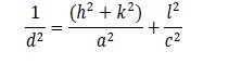
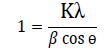
and the values are a=5.37 Å, b=5.37 Å and c=10.93 Å. The unit cell volume for tet ragonal st ructure is 315.18 Å3 calculated by formula V=a2c. The average crystal size (D) of prepared thin film was calculated from diffraction peak of (112) plane by using Debey –Scherer formula:
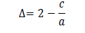
and the value was found 11.61 nm. The tet ragonal distort ion was calculated using following formula:
and the value came out to -0.033. T h e d islocat ion d ensit y ( δ ) for C u 2ZnSnS4 t h in film was calculat ed by using Williamson and Smallman’s f ormul a:
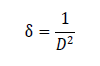
and the value is 0.007 nm-2 (Figure 1) .

Figure 1: (a). XRD spectra of Cu2ZnSnS4 film; and (b) Raman spectra of Cu2ZnSnS4 film.
Raman spectrum of a prepared Cu2ZnSnS4 thin film is shown in the Figure 1(b) . A single peak centered at Raman shift of about 331 cm-1 was detected which most likely corresponds to kesterite structure of CZTS. In the Raman spectra, no other peaks correspond to Cu2- xS, Cu2SnS3, Sn2S3, and ZnS species were detected. Therefore, the Raman spectra also supports phase purity of the CZTS thin film and free from the contaminants such as Cu2- xS, Cu2SnS3, Sn2S3, ZnS that generally found [13-18] .
Elemental composition
The elemental compositions of CZTS thin films were determined by EDS analys is and results are shown in Figure 2. A typical EDS spectrum shows peaks corresponds to Cu, Zn, Sn, and S which indicates the presence of Cu, Sn, Zn and S elements in the film. The atomic percentages of these elements are shown in the insert table of Figure 2. The low atomic/weight percentage of sulfur as compared to the theoretical values may be due to loss of sulfur content during annealing process. Therefore, to enhance compositional properties of CZTS thin films sulfurisation treatment is required [19-25].

Figure 2: EDS graph of the CZTS thin film and elemental composition in inset table.
Optical properties
Optical properties of synthesized thin film were calculated through transmittance and wavelength data taken from UVVisible spectroscopy in the 290-800 nm wavelength range. Using the Transmittance (T) data, the Absorbance (A) has been calculated using the relation:

The graph between % transmittance vs. wavelength, and absorbance vs. wavelength are displayed in Figures 3(a) and 3(b) , respect ively . Absorption coefficient ( α) of thin film can be calculated using the relation:
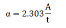
Where A and t represents absorbance and thickness of thin film, respectively. Using the above relation, the calculated value of absorption coefficient for this thin film is found ~104 cm-1 (Figure 3) . Tauc formula was used for calculat ing optical energy band gap value of these samples:
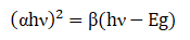
Where α,β and E g represent absorption coefficient , energy independent constant and band gap energy, respectively [26] .

Figure 3: (a). Transmittance vs. wavelength; (b) Absorbance vs. wavelength; and (c) (αhν)2 vs. (hν) graph of CZTS thin film.
The graph between h ν and (αh ν) 2 is shown in Figure 3(c) . Linear extrapolation of graph between ( h ν) and ( αh ν) 2, to h ν axis provides band gap value (Eg ) . The observed value of optical energy bad gap from above plot is found about 1.50 eV. The calculated value of band gap is comparable with known thin film solar cell band gap values (1.45-1.50 eV) , and corresponds to the absorber material's ideal band gap [27-29]. Bases on the optical properties, it can be inferred that the synthesized CZTS films are ideal for solar cell applicat ions [30] .
Surface analysis
The surface morphology of prepared thin film was observed by Scanning Electron Microscope (SEM) as shown in Figure 4. Agglomerated particles with average diameters of about 36 nm can be seen in the high magnification image shown in Figure 4(b) . Thus, the SEM images of CZTS thin film indicate that the thin film has deposited uniformly over the entire substrate. Hence, the prepared thin films may be employed as good absorber layer materials for solar cell applicat ions [31-34] .

Figure 4: SEM images of as synthesized Cu2ZnSnS4 thin film at (a) low magnification; (b) high magnification.
AFM technique was used to observe 2D and 3D micrographs of prepared CZTS thin films, and results are displayed in Figure 5 (a and b) . The surface is uniformly covered with the particles of spherical shape as shown in the micrographs (Figure 5a) . The surface seems to be flat , with a vertical height between +57.9 nm (highest ) and -49.9 nm (lowest ) . The average and Root Mean Square ( rms) roughness based on AFM micrographs were found to 1.623 nm and 2.190 nm, respectively [35] .

Figure 5: AFM micrographs for Cu2ZnSnS4 thin film (a) 2D micrograph; and (b) 3D micrograph.
Electrical properties
The hall measurements of the synthesized CZTS thin films have been performed at room temperature with magnetic field intensity of 0.556 T and a current of 0.005 mA current . The positive value of Hall coefficient revealed that synthesized thin film is a p-type semiconductor. The carrier concentration, conductivity, resistivity, and hall mobility of synthesized thin films are obtained as ~1.55 cm-3× 1016 cm-3, ~65.08 × 10⁻² Ω -1 cm-1, ~0.015 × 10² Ω cm, and ~26.1 5 cm2/Vs, respect ively [36] .
In the present work, Cu2ZnSnS4 (CZTS) thin film has been successfully prepared through spin coat ing technique using the sol -gel process. The XRD results shows the CZTS thin films having kesterite st ructure with a dominant peak at 28.7° corresponds to the plane (112) . The Raman spect rum shows a single intense peak at 331 cm-1. The absence of other Raman peaks confirms that the single phase CZTS thin film is prepared. Therefore, Raman spect ra of CZTS thin films confirm the X-ray diffract ion results. The deposited thin film shows p -type conduct ivity with absorpt ion coefficient ~104 cm-1, carrier concentration ~1.55 × 1016 cm-3, conductivity ~65.08 × 10⁻² Ω -1 cm-1, resistivity ~0.015 × 10² Ω cm and hall mobility ~26.15 cm2/Vs at room temperature. The band gap of the thin film is found about 1.50 eV which is in the good agreement with the ideal value of band gap for absorbing material. The SEM results show the uniformity of the film with average part icle size about 36 nm. The AFM micrographs show the nearly flat surface of prepared thin films. The both AFM and SEM results confirm that there are no local fractures or pinholes in the film. Therefore, the surfaces of prepared films are smooth, consistent , and tightly packed. As a result , the suggested inorganic sol -gel process offers a promising path for the quick, low cost , and large-scale production of CZTS thin films.
Mr. Jagdish Prasad is thankful to the department of Physisc, UOR, Jaipur for providing experimental and characterizat ion facilities, and department of college education, Rajsthan for allowing research in UOR, Jaipur. The authors are also thankful to MNIT MRC, Jaipur and Manipal university, Jaipur for providing characterizat ion techniques.
[Crossref]
[Crossref]
[Crossref]