In today’s world power dissipation is the main problem in digital world; this problem can be reduced by using reversible logic gates. For high performance systems, low power and smaller area are the most important criteria. Area and speed are main factors which are conflicting i.e. if speed is improving it results in larger area, hence in this paper reversible logic gates are analyzed. The power dissipation by these gates is very low; ideally their internal power dissipation is zero because these gates do not loss information. Systems where low power dissipation is required reversible logic gates will be used in place of classical logical gates like AND, OR, NAND, NOR. Reversible logic provides an alternative that may overcome many of these problems in the future. By reducing the number of reversible logic gates one can minimize the quantum cost of these gates. Reversible logic finds its application in low power CMOS, quantum computing, nanotechnology, bio-information etc
Keywords |
| Reversible logic, Reversible logic gate, quantum computing, nanotechnology. |
INTRODUCTION |
| The main aim of VLSI Circuit Design is very low power dissipation and improves system performance. According to
R.Landauer researcher there is power dissipation of KTln2 joules of heat energy per bit of information loss in classical
gates, where K is Boltzmann’s constant and T the absolute temperature at which circuit performs [1]. |
| Reversible logic does not loss any information. Reversible logic gate are the device which has n×n inputs and outputs,
its means input is equal to output or there is one to one mapping. Any gate is said to be reversible if the input can be
recovered from the output. |
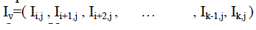
A Reversible circuit has the facility to generate a unique output vector from each input vector, and vice versa. |
| Input Vector |
 |
| Output Vector |
 |
| For each particular vector j |
| Iv⇔Ov |
| Reversible are circuits in which the number of inputs is equal to the number of outputs and there is one-to-one
mapping between vectors of inputs and outputs. |
Difference between Reversible Gate and Irreversible Gate |
| Features of reversible logic: |
| 1. One to one mapping i.e. equal no of input and output. |
| 2. For each input there is different output. |
| 3. Fan out is not allowed. |
| Features of reversible logic circuit [6]: |
| 1. Minimum number of reversible gates is used. |
| 2. Minimum number of constant inputs is used. |
| 3. Minimum number of garbage outputs should be there. |
| 4. The length of cascading gates is minimum. |
| Basic Reversible logic Gates: |
| • N= No. Of reversible logical gate used in circuit. |
| • CI= No. of inputs that are at constant 0 or 1 for synthesis of any given logical functions. |
| • GO= No. of unused outputs in reversible logic. |
TYPES OF REVERSIBLE LOGIC GATES |
| 1. Feynman Gate: It is a 2×2 reversible gate. A, B is input vector and P, Q is output vector. The output P=A,
Q=A⊕B. It is used where copying is required and inverter both at the same time due to its output. The block diagram
of this gate is shown in Fig .1 |
| 2. Double Feynman Gate (F2G): It is 3×3 Double Feynman gate. A, B, C are input vector and P, Q, R are output
vector, where P = A, Q=A⊕B and R=A⊕C. The block diagram of this gate is shown in Fig.3 |
| 3. Toffoli Gate: It is 3×3 reversible logic gate having A,B,C as input vector and P,Q ,R as output vector, where
P=A,Q=B and R=AB ⊕ C The block diagram of this gate is shown in Fig.5 |
| 4. Fredkin Gate :It is 3×3 reversible logic gate having A,B,C as input vector and P,Q,R as output vector, where
P=A,Q=A’B⊕AC , R=A’C⊕AB The block diagram of this gate is shown in Fig.8 |
| 5. Peres Gate: It is 3×3 reversible logic gate. A, B, C is input vector and P, Q, R is output vector, where P = A, Q =
A⊕B and R=AB⊕ C. The block diagram of this gate is shown in Fig.9 |
| 6. TSG gate: It is 4×4 reversible gate. A, B, C, D is input vector and P, Q, R, S is output vector, output
P = A, Q = A’C’&B’, R = (A’C’&B’) & D and S = (A’C’&B’).D⊕ (AB⊕C), the block diagram of this gate is
shown in Fig.11 |
| 7. Sayem gate: It is 4×4 reversible gate. A, B, C, D is input P, Q, R, S is output vector, where P=A, Q=A’B& AC, R=
A’B &AC& D, S=AB &A’C & D). The block diagram of this gate is shown in Fig.13 |
III. APPLICATIONS |
| Reversible logic finds its application in computer security and transaction processing, as it possess high energy
efficiency, speed and performance. |
IV. CONCLUSION |
| The paper reveals that reversible logic gates outperform classical logic gates. The prospect for further research includes
quantum computing and Nano technology. |
ACKNOWLEDGMENT |
| We take this opportunity to express our deepest gratitude and appreciation to all those who have helped us directly or
indirectly towards the successful completion of this paper. |
Tables at a glance |
 |
|
|
|
|
| Table 1 |
Table 2 |
Table 3 |
Table 4 |
Table 5 |
|
|
|
|
| Table 6 |
Table 7 |
Table 8 |
Table 9 |
|
| |
Figures at a glance |
 |
 |
 |
 |
 |
| Figure 1 |
Figure 2 |
Figure 3 |
Figure 4 |
Figure 5 |
 |
 |
 |
 |
| Figure 6 |
Figure 7 |
Figure 8 |
Figure 9 |
 |
 |
 |
 |
| Figure 10 |
Figure 11 |
Figure 12 |
Figure 13 |
|
| |
References |
- R. Landauer, “Irreversibility and Heat Generation in the Computational Process” IBM Journal of Research and Development, vol.5, pp. 183-191, 1961.
- Bennett, C.H., “Logical reversibility of Computation”, IBM Journal of Research and Development, vol.17, pp. 525-532, 1973.
- Mr. Devendra Goyal, “VHDL Implementation of Reversible Logic Gates” International Journal of Advanced Technology & Engineering Research (IJATER), Vol. 2, Issue 3, May 2012.
- Feynman, “Quantum mechanical computers”, Optics News, pp. 11-20, 1985.
- Toffoli.T, “Reversible Computing”, Tech memo MIT/LCS/TM-151, MIT lab for Computer Science, 1980.
- Vasudevan.D.P , Lala.P.K and Parkesson.J.P, “Online Testable Reversible Logic circuit Design using NAND Blocks”, Proc. Symposium on Defect and Fault Tolerance, pp. 324-331, 2004.
- E. fredkin, T. Toffoli, “Conservative Logic”, International Journal of Theory of Physics, vol.21, pp 219-253,1982.
- Md. M.h. Azad Khan, “design of full-adder with reversible gates” International conference on computer & information technology. Dhaka, Bangladesh, pp.515-519, 2002
- Bhagyalakshmi, H.R. ;.Venkatesha, M.K, “An improved design of a multiplier using reversible logic gates‟, International Journal of Engineering Science and Technology Vol. 2,pp. 3838-3845,2010.
- Michael P. Frank ,” Reversibility for efficient computing”, Ph. D. Thesis, May 1999.
- Carlin Vieri “Reversible Computing for Energy Efficient and Trustable computation”, April 1998.
|