Research & Reviews: Journal of Pure and Applied Physics
ISSN: 2320-2459
ISSN: 2320-2459
Deli Kong, Tianjiao Xin, Lirong Xiao, Xuechao Sha, Lu Yan and Lihua Wang*
Institute of Microstructure and Property of Advanced Materials, Beijing University of Technology, Beijing, 100124, China
Received: 06/03/2015 Accepted: 06/06/2015 Published: 06/08/2015
Visit for more related articles at Research & Reviews: Journal of Pure and Applied Physics
To safely and reliably use NWs for different kinds of nano devices, the structural evolution of these nanowires under external stress become very important. Here, by using the home-made in situ atomic-scale experimental device, Si nanowire bending experiments were conducted with highresolution transmission electron microscopy. The direct dynamic atomicscale observations revealed that dislocation nucleation, motion, escape and interaction were responsible for the large plastic deformation ability of Si nanowires. The prevalent full dislocation movement and interactions induced the formation of Lomer lock dislocations in the Si nanowires. We directly demonstrated that the continuous straining on the Lomer dislocations induced local atoms disordering in the Si nanowires. These results help to explain the ultra-large plastic deformation ability of Si on the nanometer scale.
Si Nanowires, Atomic-scale, in situ, Plastic deformation, High-resolution transmission electron microscopy
To safely and reliably use NWs, the mechanical properties and structural evolution of these nanowires under external stress become very important. In particular, nanowires display novel properties and functions when they are under bending strain [1-6]. Semiconductor nanowires (NWs) have been given intensive attention because of their many applications in nanotechnology, and Si NW is one of the most important types of NW since its successful fabrication. For the past decades, the studies on Si NWs have revealed a variety of “unusual deformation phenomena” compared with their bulk counterparts[5,7,8]. The results from these studies indicate that the fundamental dislocation processes in nanomaterials are considerably different than in their conventional bulk counterparts [5,7,8]. Revealing the atomic-scale deformation mechanisms of nanomaterials and controlling their elastic and plastic properties are useful for realizing the desired mechanical, physical and chemical properties [7,8]. The mechanical properties of Si NWs have been studied by many methods. With an atomic force microscopy (AFM) tip, large fracture strain was achieved by bending single Si NWs [9-11]. Using a nano- manipulator as the actuator and an AFM cantilever as the load sensor inside a scanning electron microscopy (SEM) instrument, a large tensile strain of 12% was observed [12], and an even higher elastic bending strain has been reported for Si NWs [13]. However, few structural evolution processes were related to these bending processes though these studies [9-14] that possibly involved highly active plastic dislocation events, because the fracture strains in those studies far exceeded the theoretical elastic strength limit [15,16]. Because of the lack of atomic-scale direct investigation, many of the mechanical properties of Si NWs are not known.
Here, by using the in situ atomic-scale experimental technique [17-20], the atomic-scale structural evolution processes of single Si NWs under ultra-large bending strain (exceeding 14%) were investigated in situ and recorded with high-resolution transmission electron microscopy (HRTEM). The direct dynamic atomic-scale observations revealed that dislocation nucleation, motion, escape, interaction as well as atoms disordering were responsible for ultra-large plastic strain of Si nanowires.
High-quality Si NWs with 20–50 nm in diameter and several tens of micrometers in length were synthesized with the thermal evaporation technique. The Si NWs were scattered on the previously broken TEM grid, which was covered by colloidal thin films. The scattered NWs could then be bridged on the cracked colloidal thin films (Figure 1a). The colloidal thin films shrink under electron beam irradiation and drive the nanowires to be bent (Figure 1b). The in situ bending experiments of individual NWs can then be conducted with HRTEM, and the experimental processes can be recorded at the atomic scale. The bending processes were conducted by showering an electron beam on the colloidal thin film to avoid over irradiation. The colloidal thin film shrank and bent the Si NWs continuously at a strain rate of 5.4 × 10⁻⁴/s.

Figure 1: (a) A schematic view shows that the NWs were scattered on the previously broken TEM grid, which was covered by colloidal thin films. (b) An example shows that a single NW could then be deformed by bending stress induced by the colloidal thin films under electron-beam irradiation.
Figure 2a provides a TEM image of a bend strained Si NW. According to the traditional formula εelastic = r/(r + R)% [21], where R is the bending curvature and r is the radius of the crystal Si NW, the maximum strain in the Si NW is ~1.3%. For a bent NW, the upper surface sustains the maximum tensile strain, while the bottom surface sustains the maximum compressive strain. The strain noted in the figures and the text indicates the maximum bend strain in the NW. Large number of HRTEM observations show that the synthesized NWs were defect free before the elasticity limit was reached. Figure 2b is a typical HRTEM image that corresponds to the red framed region of Figure 2a, no dislocation can be observed.

Figure 2: A low-magnification TEM images that show the bending process of a single Si NW. (b) HRTEM images of the red framed indicates the highly bent arc-shaped (111) lattices. The HRTEM image shows that no dislocation was observed before the elasticity limit was reached.
Figure 3a-c show serial TEM images showing the continuous bending process of a single Si NW. The full and partial dislocations nucleation was in situ observed (Figure 3d). For the full dislocations, they nucleated at the bottom surface of the bent NW and escaped during the deformation process. For the partial dislocation, they emission from the up-surface (under tensile strain) of the bent NW left behind an energy-cost stacking fault (Figure 3e). Partial dislocations belong to the glide set [22,23], and the activation energy of partial dislocations is much higher [24]. Partial dislocation has never been observed at room temperature in bulk Si because it always breaks at small strains (0.1%–0.2%). It is interesting to observe partial dislocation nucleation at room temperature. Here, the partial dislocation nucleation can be explained by: (a) The low dimensionality and defect-free structure make it possible for the nanomaterials to sustain high strains and high stress, which can supply enough energy to activate the dislocations, which belong to the glide sets. (b) Full dislocation glide causes the surface of the nanowire to become stepped, and stacking faults or micro-twins were observed by atomic simulation in Si with surface steps [25].

Figure 3: (a-c) Three low-magnification TEM images that show the bending process of a single Si NW. As observed in (d) and (e), the plastic dislocation events are active. (d) is enlarged HRTEM image taken from the blue framed region of (c), partial and full dislocations were observed in high strained region.
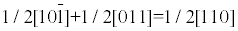
Figures 4a-4d is another example showing the continuous bending process of a single Si NW. The maximum strain in the Si NW increased from 4.9% (Figure 4a) to approximately 14.3% (Figure 4d) without abrupt failure. While Figures 4e-4h are the HRTEM images that show the in situ observation of dislocation behaviors at the atomic scale, the corresponding maximum bent strains were 2.2%, 2.6%, 4.9% and 14.3%, respectively. Figure 4e is a typical HRTEM image that captured with strain ~2.2%, indicated no dislocation can be observed before the elasticity limit. As the strain increase to be ~2.6%, full dislocation activities were observed in the bent Si NWs. In Figure 4f, a dislocation with a Burgers vector of 1/ 2[101] was nucleated at the bottom surface of the bent Si NW. These full dislocations were observed to be mobile and, therefore, have chances to interact with further straining. Figure 4g shows the in situ observation of Lomer lock dislocation formed by a dislocation reaction at the atomic scale. Local Burgers circuits were drawn to identify the Burgers vector b (b =1/ 2[110]), indicated that the nucleated is a new structural dislocation. Extra planes are seen for both ( ) and(
 ) planes. This configuration represents a Lomer dislocation (LD) [26], exhibiting the Burgers vector of
 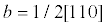 . The LD is formed by the interaction of two non-dissociated full dislocations with Burgers vectors
  and
and  , respectively, moving under applied strain on two intersecting slip planes, the
  and the
  planes. The dislocation reaction can be written as [26]:
 (1)
(1)

Figure 4: (a-d) A series of low-magnification TEM images that show the bending process of a single Si NW. Indicated that the strain sustained on the Si NW increased from 4.9% to 14.3%. No cracks were observed during the bending process. (e-h) Enlarged HRTEM images taken from the same region. The corresponding strains are 2.2%, 2.6%, 4.9% and 14.3%, respectively.
With continuous straining, these locks could not be unzipped, and the locked lattice regions became disordered, leading to atoms disordering. Figures 4h shows the in situ observation of LD formation and the subsequent atoms disordering process at the atomic scale. As shown, the region of the LD lock became lattice disordered as the strain increased. The LD junction was expected to be sessile because it can glide in neither of the slip planes of the reactant dislocations. This sessile dislocation will make the local stress very high as the strain increases and the lattice disordering was more likely to happen in this area.
In summary, the in situ atomic-scale observation shows that the ultra-large bent straining of Si nanowires involves highly activated plastic dislocations. Both the partial and full dislocations were observed at room temperature in plastic deformed Si NWs. The dislocation nucleation, motion; dislocations interaction led to the formation of Lomer locks; strain-induced disordering that caused by the continuous straining on sessile Lomer dislocations are all responsible for plastic deformation ability of nanosize Si NWs.
This work was supported by the Key Project of C-NSF (50831001), the NSF (10102001201304) and the Beijing Nova Program (XXJH2015110), the Beijing PXM201101420409000053 and Beijing 211 Project. Specialized Research Fund for the Doctoral Program of Higher Education of China 3C102001201301). The Project of Construction of Innovative Teams and Teacher Career Development for Universities and Colleges under Beijing Municipality (IDHT20140504).