International Journal of Advanced Research in Electrical, Electronics and Instrumentation Engineering
ISSN ONLINE(2278-8875) PRINT (2320-3765)
ISSN ONLINE(2278-8875) PRINT (2320-3765)
V.N.Lakshmi1, KambeBalaji Rao2
|
| Related article at Pubmed, Scholar Google |
Visit for more related articles at International Journal of Advanced Research in Electrical, Electronics and Instrumentation Engineering
This paper presents a high efficiency step-upDC-DC converter for low-DC renewable energy sources.The proposed DC-DC converter is controlled byasymmetrical pulse width modulation(APWM) techniqueand achieves Zero-current switching(ZCS) of all outputdiodes. Compared to the previous DC-DC converters, thevoltage stresses of the semiconductor devices can be reducedin the proposed converter. Simulation results areobtained from a 200 W output power. The proposed DC-DCconverter achieves a high efficiency of 97.5 % at the ratedload.Further project has been extended to three phase grid tie inverter using sinusoidal pulse width modulation technique.
Keywords |
| DC-DC converter, soft-switching, highvoltage gain, zero-current switching(ZCS),Three Phase Inverter |
INTRODUCTION |
| The power generation systems using low-DCrenewable energy sources such as photovoltaic moduleand fuel cell need a high step-up DC-DC converter tointerface the low-DC voltage to the high DC voltagedistribution network [1]. Lots of efforts have been madeto develop high step-up DC-DC converters with a highefficiency [2]-[6]. Among the investigated topologies, theactive-clamped step-up DC-DC converters in [4]-[6] aregaining its popularity, thanks to its high step-up ratio andsoft-switching operation. The active-clamped step-upDC-DC converters in [4]-[6] has a high step-up gain byusing the active-clamp circuit at the primary side and thevoltage doubler rectifier at the secondary side. Moreover,the series-resonance between the transformer leakageinductor and the capacitor in the voltage doubler rectifiermakes the output diodes to be turned off at zero currentcondition [5]. However, the power switches at theprimary side operate under hard-switching condition,which still causes high switching power losses and highheat dissipation problems. The half-bridge dc-dcconverter has been presented to reduce switching powerlosses at highvoltage side [1]. The output diodes areturned off at zero current by using the voltage doublerrectifier. However, an additional half-wave rectifier isneeded, which increases switching power losses.In order to overcome these problems, this paperproposes a high-simulation efficiency dc-dc converter for low-dcrenewable sources. An improved activeclamped dc-dcconverter is presented by using a dual active-clamping circuit. The voltage stress of power switches can bereduced at primary side. The performance of the proposedconverter is verified using a 200 W simulation prototype. The simulation results confirm that a highefficiency of 97.5 % is achieved at 50 V input voltage for200 W output power with an improved dynamic performance. |
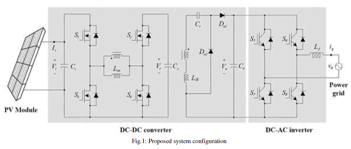
| In this paper a new DC-DC converter topology is proposed to step up the fuel cell voltage and provide a stable dc-link for the DC-AC inverter. The proposed DC-DC power conversion unit consists of a two parallel connected buck-boost converters. This produces an independently controllable dual voltage output. Block diagram of proposed converter is shown in Fig.1. As it will be shown the use of the proposed topology along with a DC-AC inverter eliminates the need for a transformer to provide the required voltage gain. As a result, proposed topology has the following advantages: |
| ïÃâ÷ Operates from a single input voltage |
| ïÃâ÷ No transformer is required to achieve a voltage gain of 5 in per unit |
| ïÃâ÷ If a single phase is connected at its output the system can generate 230VAC output from a 50VDC input source without the use of a transformer. |
 |
INVERTER CONTROL SCHEME |
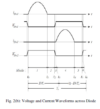
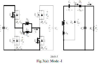
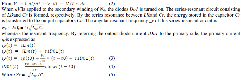
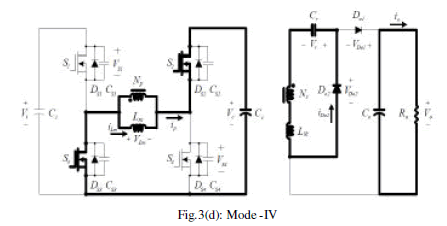
| The Fig. 1 shows the circuit diagram of the proposed stepupDC-DC converter. This converter combines an inputcapacitor Ci, a clamp capacitor Cc, main switchesS1 andS4, an auxiliary switchesS2 and S3, the resonant capacitorCr, two output diode Do1 and Do2, an output capacitor Co,and the secondary side leakage inductor Llk. Each switchhas its own parasitic capacitor CS1 ~ CS4 and body diodeDS1 ~ DS4. The switches operate at a constant switchingperiod Ts(= 1/fs) with the asymmetrical pulse-widthmodulation(APWM). The transformer T has themagnetizing inductor Lm and leakage inductor Llkwith theturns ratio of 1 : N where N = Ns/Np. The proposedconverter operates in a continuous conduction mode sothat the magnetizing inductor current iLmflowscontinuously. The capacitors Cc, Co are large enough sothat their voltages are considered constant as Vcand Vo. Dis the duty ratio based on S1 (S4) turn-on time. Fig. 2(a)shows the operation waveforms of the primary sidecomponents. Fig. 2(b) shows the operation waveforms ofthe secondary side components. Fig. 3 shows theoperation modes of the proposed converter for Ts. The proposed converter has six distinct operating modes forTsas follows: |
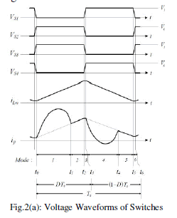 |
| Mode 1 [t0, t1]: At t = t0, S1 and S4 are turned on. Since VLm= Vi, the magnetizing inductor current iLmincreases linearly as |
 |
 |
 |
| Mode 2 [t1, t2]: At t = t1, the half-resonant period for the output diode currents iDo1 is finished. The output diode currents iDo1 is zero before Do1 is turned off. Zero current switching of Do1 is achieved without any diode reverse recovery problem at the end of Mode 2. |
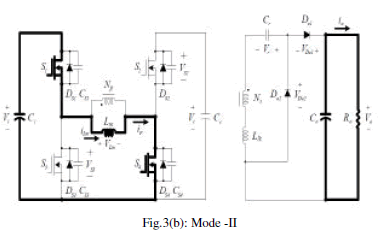 |
| Mode 3 [t2, t3]: At t = t2, S1 and S4 are turned off. The primary current ipcharges CS1 and CS4, discharges CS2 and CS3. The voltage VS1 across S1 increases from zero to the voltage Viand The voltage VS4 across S4 increases from zero to Vc. Since the capacitor CS (= CS1 = CS4) is very small, the time interval during this mode is considered negligible compared to Ts. |
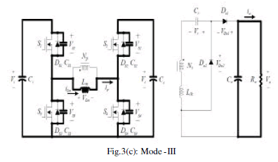 |
| Mode 4 [t3, t4]: At t = t3, the auxiliary switches S2 and S3 are turned on with zero voltage. Thus, switching loss is reduced. Since VLm= –Vc, the magnetizing inductor current iLmdecreases linearly as |
 |
| When –nVcis applied to the secondary winding of Ns, the output diode Do2 is turned on. The series-resonant circuit consisting of Llkand Cr is formed, respectively. Through the output diode Do2, the energy is transferred to the resonant capacitor Cr. By referring the output diode current iDo2 to the primary side, the primary current ipis expressed as |
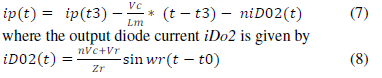 |
| Mode 5 [t4, t5]: At t = t4, the half-resonant period of the output diode currents iDo2 is finished. The output diode current iDo2 is zero before Do2 is turned off. Zero-current switching of Do2 is achieved without any diode reverse recovery problem at the end of Mode 5 |
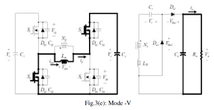 |
| Mode 6 [t5, t6]: At t = t5, S2 and S3 are turned off. The primary current ipcharges CS2 and CS3, discharges CS1 and CS4. The voltage VS2 across S1 increases from zero to the voltage Vcand The voltage VS3 across S3 increases from zero to Vi. Since the capacitor CS (= CS2 = CS3) is very small, the time interval during this mode is considered negligible compared to Ts. The next switching cycle begins when S1 is turned on again. By imposing the voltagesecond valence role on the magnetizing inductor Lm, the capacitor voltages Vc, and Vrcan be expressed as |
 |
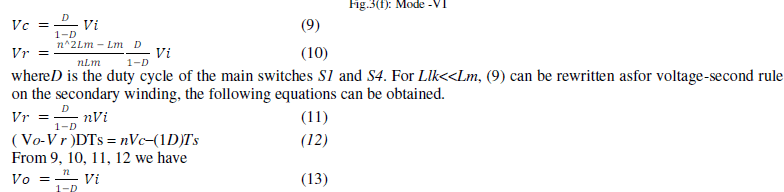 |
| The maximum voltage stress of S1 and S3 is confined to the input voltage Vi. The voltage stress of S2 and S4 is confined to the clamping capacitor voltage Vc. Fig. 4 shows the relation between the clamping capacitor voltage Vcand the duty ratio D. The dual active-clamping circuit is used in the proposed converter. The clamping capacitor voltage in case of the dual active-clamping circuit is always lower than the clamping capacitor voltage in case of the conventional active-clamping circuit. It means that the switch voltage stress of the proposed converter is always lower than the switch voltage stress of the previous converter [4] using the conventional active-clamping circuit. Especially, when the duty ratio is below 0.5, the clamping capacitor voltage can be lower than the input voltage Vi. It is critically beneficial in low-voltage PV applications where more than 50 % of the power losses are lost as switching power losses. The output diode currents iDo1 and iDo2 should be zero. |
SIMULATIONRESULTS |
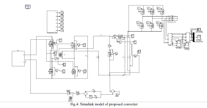
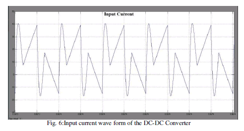
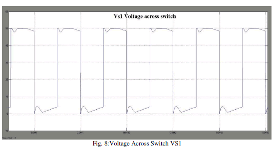
| Fig. 4 shows the Simulink model of the proposed converter and Fig. 5, 6 shows the primary current ipand output voltage of DC-DC converter, Fig. switch voltagesVS1 and VS3 for 200 W output power. Fig. 5shows the simulation waveforms at 50 V input voltage.As shown in Figs. 5, VS1 and VS3 are clamped at the inputvoltage. Fig. 6 shows the primary current ip, clampingcapacitor voltage Vc, and switch voltages VS2 and VS4 for200 W output power. Fig. 6 shows the simulationwaveforms at 50 V input voltage. The clamping capacitorvoltage Vcis 48 V. VS2 and VS4 are clamped at 48 V.Fig. 8 shows the measured power efficiencies of theconverters at 50 V input voltage for different output loadconditions. The proposed converter achieves theefficiency of 97.5 % for 200 W output power. Theprevious active-clamped converter achieves the efficiencyof 97.2 % for 200 W output power. The efficiency of 0.3% is improved by the proposed converter at 50 V inputvoltage for 200 W output power. The previous halfbridgeconverter achieves the efficiency of 97.0 % for200 W output power. The proposed converter achievesthe highest efficiency for the rated output power.Switching power losses are reduced by decreasing thevoltage stress of power switches in the proposedconverter. The power efficiency is increased by reducingswitching power losses. |
 |
 |
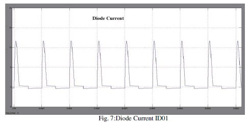
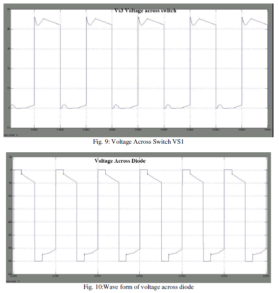
| Fig. 7 shows the simulation waveforms for 200 W output power. The diode currentflows in a resonant manner by the series resonance between the leakage inductor and the resonant capacitor. The diode current is zero before the output diode isturned off. Zero-current switching of each output diode isachieved at its turn-off instance. |
 |
 |
 |
| Fig. 8 shows the output diode voltages VDo1 and VDo2and output diode currents iDo1 and iDo2 for different outputload conditions. The switching powerloss caused by the diode reverse recovery current can beremoved by zerocurrent turn-off of the output diode. |
 |
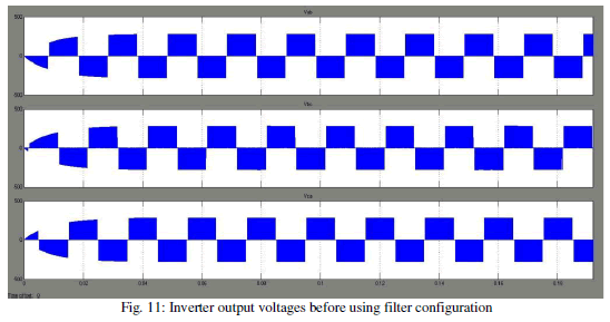 |
| Fig. 11 shows the output voltage of inverter and output voltage without filterfor different outputload conditions. The switching powerloss caused by the switching of three phase inverter causes the output voltage to be stepped waveform. |
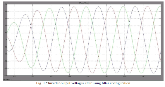 |
| Fig. 12 shows the output voltage of inverter and output voltage with filterfor different outputload conditions. The switching powerloss caused by the switching of three phase inverter causes the output voltage to be stepped waveform without filter and filtering causes the output voltage to be pure sinusoidal which is directly fed to the grid. |
CONCLUSION |
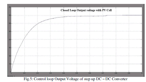
| This paper presents a high efficiency step-up DC-DCconverter for low-DC renewable energy sources. Theoperation of the proposed converter has been described.The simulation results has been presented at inputvoltage Vi= 50 V. The proposed converter reduces theswitching power losses, increasing power efficiency. Byusing series resonant circuit, the proposed converterachieves ZCS turn-off to remove the reverse-recoveryproblem on output diodes. Simulation results haveshown that the proposed converter achieves a high efficiency of 97.5 %. By feeding DC output voltage of converter to three phase grid tie inverter gives pure sinusoidal voltage with 50Hz frequency and suitable output AC voltage . |
References |
|