Research & Reviews: Journal of Pure and Applied Physics
ISSN: 2320-2459
ISSN: 2320-2459
Usha Shukla*, Suraj Sharma
Department of Applied Sciences, Amity University Uttar Pradesh, Uttar Pradesh, Lucknow, India
Received: 10-March-2022 Manuscript No. JPAP-22-56787; Editor assigned: 14- March-2022 Pre QC No. JPAP-22-56787(PQ); Reviewed: 24-March-2022, QC No. JPAP-22-56787; Accepted: 28-March-2022, Manuscript No. JPAP-22-56787(A) Published: 31-March-2022, DOI:10.4172/2320-2459.10.1.005.
Visit for more related articles at Research & Reviews: Journal of Pure and Applied Physics
At the hour of composing, optoelectronic gadgets have found out their way into a wide range of parts of current life whether it be the universal marker LEDs, TVs, PCs, strong state lighting and innumerable different things or in the scanner tag examining frameworks at the general store, minimized circle (CD), Digital Versatile Disc (DVD) and blue-beam frameworks at home, the laser printer in the workplace, or when utilizing a phone or watching satellite TV. Ludicrous decade or so there has been a data blast whereby data from everywhere the world can be immediately gotten to by anybody with an Internet-empowered gadget. In these applications, it is a semiconductor-based optoelectronic gadget that shapes a fundamental piece of the framework. These gadgets incorporate sources, for example, Light-Emitting Diode (LEDs) and laser diodes, photo detectors, optical speakers, and optical modulators. With such gadgets, one can create, balance, identify, and change photons in a practically equivalent to approach to electrons in an electrical web of circuit. In this review we are considering the fundamental actual associations among electrons and photons that happen in semiconductors and how they might be outfit to deliver a wide assortment of gadgets.
LED;Photo detector; Integrated detector;Photo diode; Solar cell
Optoelectronics is the correspondence among optics and gadgets which incorporates the investigation, plan and production of an equipment gadget that changes over electrical energy into flash and light into energy through semiconductors. This gadget is produced using strong glasslike materials which are lighter than metals and heavier than separators. Optoelectronics gadget is essentially an electronic gadget including light. Figure 1 shows the optoelectronics gadget. This gadget can be found in numerous optoelectronics applications like military administrations, broadcast communications, programmed admittance control frameworks and clinical supplies.

Figure 1: Optoelectronics gadget can be found in numerous optoelectronics applications like military administrations, broadcast communications, programmed admittance control frameworks and clinical supplies.
This scholarly field covers a wide scope of gadgets including LEDs and components, picture get gadgets, data shows, optical correspondence frameworks, optical stockpiles and far off detecting frameworks, and so forth Instances of optoelectronic gadgets incorporate telecom laser, blue laser, photograph diodes, driven traffic signals, optical fiber and sunlight based cells. Larger part of the optoelectronic gadgets (direct change among electrons and photons) are Light Emitting Diodes, laser diodes, photograph diodes and sun based cells.
Optoelectronic gadgets have been made conceivable simply because of synchronous improvements in gadget ideas and plans, gem development methods with super fine power over the material structures and thickness, and furthermore settling some principal materials-related issues like doping. Vital are light producing diodes and lasers while working on various standards (unconstrained discharge and animated outflow, individually) the recorded improvements related with these two gadgets are firmly related and can't be decoupled. Lasers are utilized for broadcast communications, strong state laser siphoning, standardized tag checking, materials handling, optical information stockpiling, exploration, and clinical diagnostics while light producing diodes are liked for shopper gadgets, traffic lights, auto, strong state and fluid precious stone showcases, and particularly appealing for 'lighting impacts' that need various degrees of shading blending.
Light emission in semiconductors
The main report on Light-Emitting Diode (LEDs) traces all the way back to 1907, when distributed. A Note on Carborundum [1], anyway the disclosure and improvement of the hypothesis and comprehension of p-n intersections in semiconductor materials enveloping the premise of present gadgets didn't occur until not many years after the fact. Semiconductor p-n intersections were first (coincidentally) framed and found by R. Ohl in 1940 and announced in 1947. Glow from Ge and Si intersection diodes was seen as ahead of schedule as 1952. Be that as it may, Ge and Si were helpless light producers due to the aberrant bandgap. The significance of direct bandgap semiconductors for productive radioactive recombination was first distinguished by Bardeen in 1956 [2]. In less than 10 years, four examinations bunch freely revealed the principal p-n intersection lasers.
H. Kroemer and Z. I. Alferov won the 2000 Respectable Prize in Material science for their work on Twofold Heterojunctions (DHs), for transporter and optical restriction to accomplish constant activity at raised temperatures. Exhibition of lasing at room temperature utilizing DHs was accounted for all the while by two gatherings. Dupuis et al. shown the first hetero structure laser dependent on upper lattices (GaAs/AlGaAs) with qualities similar to those of customary DHs lasers in 1978 [3].
The following innovation forward leap for semiconductor-based lasers was the applied turn of events and exploratory acknowledgment of pseudomorphic or stressed objects that would diminish the edge current esteem subsequently bringing about higher yield power. Figure 2 shows the semiconductor laser. While quantum dab lasers in research labs have shown properties better than those of quantum well lasers, business Light Emitting Diodes and lasers are still generally dependent on quantum well model. Another laser idea, the Quantum Course Laser (QCL) [4] proposed by Capasso et al. in the mid- 1990s was made conceivable by the fine control got with MBE of slim hetero structure layers. It depends on bound electrons for light outflow inside a grouping of various slim quantum wells rather than band to band recombination in the mass material, with a more extensive scope of frequency tuning (4–19 μm).

Figure 2: Semiconductor laser hypothetically considered the benefits of utilizing quantum boxes as well as quantum spots in lasers.
Crystal growth techniques
AlGaAs-GaAs was one of the underlying frameworks with direct bandgap researched for the producing layer of hetero structure gadgets due to the conceivable high productivity yet development with deformity free limits was at first acquired exclusively by fluid stage epitaxy. The advancement of atomic pillar epitaxy and Metal Natural Substance Fume Statement (MOCVD) strategies in 1970s gave sharp hetero interfaces better exactness in piece and thickness control.
Utilizing MOCVD Dupuis et al. revealed the main room temperature beat activity of AlGaAs DHs laser just as the principal quantum well laser with execution coordinating with that of a standard DH laser. After the original work of Arakawa et al., MOCVD and MBE were additionally used to develop quantum spots in InAs/GaAs grid confounded framework utilizing the Stranski–Krastanow development mode. In any case MOCVD is the development procedure reasonable for huge territory substrates, by and large expense, and presently broadly utilized by the optoelectronics business as a rule.
The primary apparent LED was exhibited utilizing GaAsP compound semiconductor by Holonyak in 1962. In the mid-1960s his gathering built up the fume stage epitaxy (VPE) development of GaAsP also, GaAsP heteroepitaxy on GaAs substrates, the initial move toward business LEDs. For apparent LEDs, GaAsP amalgams would be supplanted by AlGaAs due to the direct bandgap in the apparent locale of the electromagnetic range and grid coordinated to GaAs substrate. The more extensive bandgap empowered effective heteroepitaxial gadget plans. With high virtue AlGaAs layers, AlGaAs-based LEDs overwhelmed the apparent LED market to turn into the primary high splendor red LEDs to be utilized in auto industry. While research moved towards hetero structures for productive LEDs and lasers, there was a requirement for ID of grid coordinated hetero structures over a scope of emanation frequencies. In 1970 the principal semiconductor quaternary gadget utilizing AlGaAsP-GaAsP heterojunctions was illustrated, demonstrating that quaternary III-V mixtures could offer bandgap tuning in cross section coordinated with heterojunctions. InAlGaP turned into the following material arrangement of interest for high productivity apparent LEDs. Some of strong state business LEDs are truth be told dependent on this material framework.
In the mid-1980s material quality and p-type doping in GaN were inexplicable issues for creation of productive light emanating p-n intersections [5]. In 1986, Akasaki et al. showed a two-venture MOCVD development measure for low imperfection thickness GaN on a low temperature AlN cushion. In the interim, fruitful p-type doping of GaN was exhibited utilizing Mg. It turns of events driven Nakamura to show the first brilliant GaN-based blue LEDs following twenty years of the first report to start the business strong state lighting period [6]. The revelations on optical gadgets and advances on dynamic compound semiconductor materials have covered an enormous segment of the electromagnetic range from the apparent to the far infrared.
Photo detectors
Photo detectors are optoelectronic gadgets that convert the optical energy into an electrical sign. They rely upon the characteristic material properties (eluded as retention edge) and can have inner increase. The least complex type is the photoconductor where the dynamic conductivity increments by the occurrence photons, however its exhibition is restricted by warm clamor (enormous dim current).
The p-n intersection photodiode is the most broadly recognized sort utilized for all applications in every single material framework, where the energy of photons assimilated is equivalent to the material bandgap energy. The rule is based on assimilated photons in the opposite predisposition district of the p-n intersection making electron–opening sets, and subsequently adding to the electrical current. In the occasion that there is inward increase the photocurrent can be enhanced. Photodiodes are fundamental for all applications that require light identification with low commotion: from motor observing to cosmology. In correspondence frameworks photodiodes have applications in high and low force identification, radio-over-fiber transmission, stage exhibit radar, photonic simple to computerized converters (ADCs), and stable microwave signal age. Perception of photovoltaic impact in p-n intersections was first revealed by R. Ohl in 1941. The primary p-n photodiodes were made of silicon furthermore, germanium, due to their inborn material properties.
Germanium precious stones were cooled (at 77 K) to decrease dim flows with restricted use in spectroscopy. After Anderson's report of Ge-GaAs heteroepitaxy, p (Ge)-n (GaAs) heterojunction diodes were illustrated for infrared discovery. Around then heteroepitaxy of Ge on Si substrates was not viewed as an option on the grounds that the 4.2% grid confuse between the two materials brought about high separation thickness joined with surface harshness and forestalled further improvement as needed for reconciliation with hardware. Rather II-VI or III-V materials in ternary or quaternary structures for heterojunction p-n photodiodes have been created for various frequencies furthermore, applications [7].
For extremely low degrees of optical sign photo detectors with inside acquire are liked. Torrential slide photo detectors (APDs) have enormous addition because of the effect ionization measure at breakdown voltage while phototransistors show inner increase without inclination reliance [8].
Integrated optoelectronics
The main idea of optoelectronic incorporated circuits was proposed in the last part of the 1960s however down to earth showings required a very long time to acknowledge on the grounds that exclusively advanced segments when amassed together for a particular application could in any case beat a solidly incorporated chip. Solely after normal substrates, for the most part of protecting kind for decreased parasitic reactance related with more limited holding wire inductances and more modest capacitors, PC helped plan for circuit, and progressed handling methods, solid optoelectronic coordinated circuits began performing or beating 'half breed optical incorporated circuits'. At the point when the joining included components like optical waveguides, optical couplers, with light sources and locators for signal coordination and circulation minus any additional preparing all through electronic circuits, this solid combination were eluded as Photonic Incorporated Circuits (PICs).
Integrated light sources
During the 1970s and 1980s the steady advancement made in optical fiber correspondences innovation too empowered the quest for semiconductor gadgets that could improve transmission, gathering and handling of optical signs including coordinated arrangements. The principal exhibitions of semiconductor lasers on semi insulating substrates viable to single mode optic fiber were before long followed by reports of incorporation of semiconductor lasers with improved on hardware (semiconductors) as driver circuit. Be that as it may, in 1986 the solid coordination of an electro absorption modulator and a quantum well laser working at 1.55 μm end up being the effective way to deal with date. Electro absorption modulators depend on either the Franz-Keldysh impact if there should be an occurrence of mass material or the quantum kept obvious impact (QCSE) for structures with quantum control [9]. The main electro absorption optical modulator dependent on FranzKeldysh impact was shown in 1976. Electro Absorption (EA) modulators are basic, smaller, and productive semiconductor gadgets in overseeing information transmission as well as having a design viable for incorporation with DH semiconductor lasers. Their innovation has been refined regarding handling with epitaxial regrowth, bundling, and advancement for business items in the twenty-first century.
Integrated detectors
The plan of an incorporated locator is constrained by outer framework level boundaries relying upon explicit applications, for instance, in information correspondences acquiring the most minimal electrical commotion while keeping the amplest electrical transmission capacity of the post hardware, quick obtaining time, and straightforwardness to the information design. With a wide range of decisions for identifiers and semiconductor hardware, the fundamental plan for mix depends on tradeoffs between the indicator execution (optical affectability and electrical transfer speed) and the electronic handling hardware (preamplifier, post enhancer) just as light coupling into the gadget. For optical fiber correspondences in 1970 the beneficiary plan perspectives were tended to by Personick, followed by reports of incorporation on similar substrate for various segments and photo detectors with various semiconductors [10]. Just in the mid-1990s In P-based long frequency solidly incorporated optical recipients with p-I-n finders and heterojunction bipolar semiconductors dominated the presentation of half breed beneficiaries. To date because of the cutting edge innovation improvement for CMOS and hardware in general, the thickness of incorporation among photonics and hardware vary by a few significant degrees.
One special case is the showing of In P-based photonic incorporated circuits for huge amassed information in optical interchanges applications [11]. Another is for imaging CMOS-based incorporated locators based on Charge Coupled Gadgets (CCDs) as demonstrated. The idea at Ringer Labs began in 1969, and later formed into models for imagers [12]. CCDs showed high affectability and low commotion for applications in high goal cosmology and high goal instrumentation. Thusly its applications promoted into scanners, computerized cameras, and standardized identification pursuers.
Optical interconnects
In the last part of the 1960s after work distributed by Smith a few examinations began utilizing optics for computerized rationale entryways. The insight was that the speed of CMOS-based circuits would be chiefly restricted by interconnection delays rather than entryway delay with the diminishing element sizes. With the interest for more extensive optical transfer speed also, expansion in electronic chip territory, circuits and frameworks fashioners began searching for various other options.
For the accompanying twenty years (1970–1980s) the mission for optical figuring and optical advanced doors proceeded just as fast advancement in optical fiber correspondence limit and epitaxial materials. The idea of Vertical-Pit Surface-Radiating Laser (VCSEL) was created in 1977 by Iga and collaborators and revealed in 1979 [13]. This unique class of semiconductor lasers can have extremely low worth of limit current, in a more limited cavity, more modest dynamic territory, and more modest volume than traditional strip lasers. The solid creation and simple gadget partition without the requirement for wonderful dividing (against edge transmitting) additionally showed that VCSELs could be a promising innovation for coupling to resemble optical filaments or vertical combination with photo detectors in an exhibit mode.
Both VCSELs and electro absorption modulators in optical correspondences offered new alternatives as multidimensional varieties of optical gadgets: VCSELs in optical information joins (brief distances) and modulators coordinated with lasers (significant distances). Particularly GaAs-based VCSELs empowered equal preparing as optical interconnects offering an option for more extensive amassed bit rate limit than electrical interconnects without the limits of impedance coordinating, segregation, and constriction notwithstanding more modest structure factor and lower absolute electrical force scattering. In 2012, IBM declared 1 Tb/s information equal exchange limit utilizing a coordinated GaAs-based VCSEL chip with 24 transmitters and 90 nm CMOS innovation collectors in 150 m short connection [14].
Types of optoelectronics devices
Light absorption and emission: An enormous number of optoelectronic gadgets comprise of a p-type and n-type area, actually like a standard p-n diode. The key contrast is that there is an extra collaboration between the electrons and openings in the semiconductor and light. This collaboration isn't confined to optoelectronic gadgets. Ordinary diodes are likewise known to be light touchy and at times additionally discharge light. The key contrast is that optoelectronic gadgets, for example, photodiodes, sunlight based cells, LEDs and laser diodes are explicitly intended to streamline the light retention and outflow, bringing about high change proficiency.
Light retention and emanation in a semiconductor is remembered to be intensely reliant upon the nitty gritty band construction of the semiconductor. Direct bandgap semiconductors, i.e. semiconductors for which the base of the conduction band happens at the equivalent wave vector, k, as the limit of the valence band, have a more grounded assimilation of light as described by a bigger retention coefficient. They are likewise the supported semiconductors when creating light emanating gadgets. Backhanded bandgap semiconductors, for example semiconductors for which the base of the conduction band doesn't happen at the equivalent wave vector as the limit of the valence band, are known to have a more modest ingestion coefficient and are seldom utilized in light radiating gadgets.
This striking contrast is additionally represented with Figure 3 and can be clarified dependent on the energy and force preservation needed in the electron-photon connection. The direct bandgap semiconductor, which has a vertically adjusted conduction and valence band, is appeared in Figure 3a. Retention of a photon is acquired if an unfilled state in the conduction band is accessible for which the energy and force approaches that of an electron in the valence band in addition to that of the occurrence photon. Photons have little force relative of their energy since they travel at the speed of light. The electron in this way makes a practically vertical progress on the E-k graph.

Figure 3: E-k diagram showing (a) Photon absorption in a direct bandgap semiconductor (b) Photon absorption in an indirect bandgap semiconductor assisted by phonon absorption and (c) Photon absorption in an indirect bandgap semiconductor assisted by phonon emission.
For a roundabout bandgap semiconductor, the conduction band isn't vertically adjusted to the valence band as demonstrated in Figure 3b. Consequently a just cooperation of an occurrence photon with an electron in the valence band won't give the right energy and force comparing to that of an unfilled state in the conduction band. Therefore retention of light needs the support of another molecule, to be specific a photon. Since a phonon, i.e. a molecule related with grid vibrations, has a generally low speed near the speed of sound in the material, it has a little energy and huge force contrasted with that of a photon. Preservation of both energy and force can consequently be acquired in the retention cycle if a phonon is made or a current phonon partakes. The phonon helped assimilation measures are delineated with Figure 3b and 3c.
Figure 3(b) delineates the retention of a photon supported by the concurrent ingestion of a phonon, while Figure 3(c) portrays the assimilation of a photon, which brings about the emanation of a phonon.
The base photon energy that can be assimilated is somewhat underneath the bandgap energy on account of phonon ingestion and must be marginally over the bandgap energy on account of phonon outflow. Since the ingestion cycle in an aberrant bandgap semiconductor includes a phonon notwithstanding the electron and photon, the likelihood of having a collaboration occur including every one of the three particles will be lower than a straightforward electron-photon communication in a direct bandgap semiconductor. Therefore one finds that ingestion is a lot more grounded in a direct bandgap material.
Likewise, on account of light emanation, a direct bandgap material is additionally bound to radiate a photon than a roundabout bandgap material. While roundabout bandgap materials are sporadically utilized for certain LEDs, they bring about low transformation effectiveness. Direct bandgap materials are utilized only for semiconductor laser diodes.
Photodiodes
Photodiodes and glasslike sun oriented cells are basically equivalent to the p-n diodes, which have been depicted in this part. In any case, the diode is presented to light, which yields a photocurrent notwithstanding the diode current with the goal that the absolute diode current is given by:
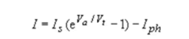
Where the extra photocurrent, Iph is because of photo generation of electrons and openings appeared in Figure 4. These electrons and openings are maneuvered into the district where they are larger part transporters by the electric field in the consumption locale.

Figure 4: Motion of photo-generated carriers in a p-n photodiode.
The photograph produced transporters cause a photocurrent, which goes against the diode current under forward predisposition. Along these lines, the diode can be utilized as a photo detector - utilizing a converse or even zero inclination voltage - as the deliberate photocurrent is relative to the episode light power. The diode can likewise be utilized as sunlight based cell - utilizing a forward inclination – to create electrical force. The essential attributes of a photodiode are the responsivity, the dull current and the transmission capacity. The responsivity is the photocurrent partitioned by the occurrence optical force. The most extreme photocurrent in a photodiode approaches.
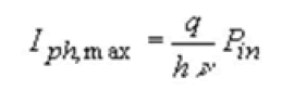
Where Pin is the episode optical force. This greatest photocurrent happens when every approaching photon makes one electron-opening pair, which adds to the photocurrent. The most extreme photocurrent within the sight of a reflection, R at the outside of the photodiode and ingestion over a thickness d, in a material with a retention coefficient, a, is given by:
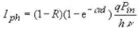
This photocurrent is gotten by incorporating the age rate over the retention district with thickness, d. The photocurrent is additionally diminished if photograph produced electron-opening sets recombine inside the photodiode as opposed to being cleared into the locales where they are larger part transporters.
The dim current is the current through the diode without light. This current is because of the ideal diode current, the age/recombination of transporters in the exhaustion area and any surface spillage, which happens in the diode. The dim current clearly restricts the base force distinguished by the photodiode, since a photocurrent a lot more modest than the dim current would be difficult to quantify.
In any case, the genuine constraint is the shot commotion created by the current through the diode. The shot commotion as evaluated by the normal of the square of the clamor current is given by:
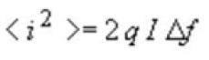
Where I is the diode current and Df is the transfer speed of the indicator. The transfer speed of the diode is influenced by the travel season of the photograph produced transporters through the diode and by the capacitance of the diode. The transporter travel time yields the inborn transfer speed of the diode while the capacitance along with the impedance of the intensifier or the transmission line associated with the diode yields a the parasitic RC delay.
Solar cells
Sun based cells are ordinarily enlightened with daylight and are planned to change over the sun oriented energy into electrical energy. The sun oriented energy is as electromagnetic radiation, all the more explicitly "dark body" radiation as portrayed in segment. The sun's range is predictable with that of a dark body at a temperature of 5800 K. The radiation range has a top at 0.8 eV. A critical piece of the range is in the noticeable scope of the range (400 - 700 nm). The force thickness is roughly 100 mW/cm2.
Just piece of the sun powered range really makes it to the world's surface. Dispersing and ingestion in the world's air, and the occurrence point influence the episode power thickness. Consequently, the accessible force thickness relies upon the time, the season and the scope of a particular area. Of the sun based light, which arrives at a sun oriented cell, just photons with energy bigger than the energy bandgap of the semiconductor create electron-opening sets. Moreover, one tracks down that the voltage across the sun oriented cell at where it conveys its most extreme force is not exactly the bandgap energy in electron volt. The general force transformation effectiveness of single-glasslike sunlight based cells goes from 10 to 30% yielding 10 to 30 mW/cm2.
The computation of the greatest force of a sun oriented cell is delineated by Figure 5 and Figure 6. The sign show of the current and voltage is appeared also. It considers a flow emerging from the cell to be positive as it prompts electrical force age. The force produced relies upon the sunlight based cell itself and the heap associated with it. For instance, a resistive burden is appeared in the chart beneath.

Figure 5: Circuit diagram and sign convention of a p-n diode solar cell connected to a resistive load.

Figure 6: The current and the power as function of the forward bias voltage across the diode for a photo current of 1 mA
We distinguish the open-circuit voltage, Voc, as the voltage across the enlightened cell at zero current. The short out current, Isc, is the current through the enlightened cell if the voltage across the cell is zero. The short out current is near the photocurrent while the open-circuit voltage is near the turn-on voltage of the diode as estimated on a current scale like that of the photocurrent.
The force rises to the result of the diode voltage and current and from the start increments directly with the diode voltage yet then quickly goes to zero as the voltage moves toward the turn-on voltage of the diode. The greatest force is gotten at a voltage named as Vm with Im being the current at that voltage.
The fill factor of the sunlight based cell is characterized as the proportion of the greatest force of the cell to the result of the open-circuit voltage, Voc, and the short out current, Isc, or:
LEDs
Light creating diodes are p-n diodes in which the collection of electrons and openings yields a photon. This recombination of radioactive measure happens chiefly in direct bandgap semiconductors where the most decreased conduction band least and the most critical valence band most prominent occur at k=zero, where k is the wavenumber. Occasions of direct bandgap semiconductors are GaAs, In P, and GaN while most assembling IV semiconductors including Si, Ge and SiC are underhanded bandgap semiconductors.
The recombination of radioactive measure is in competition with non-radioactive recombination cycles, for model, trap-helped recombination. Radioactive recombination rules at high minority transporter densities. Using a quantum well, a slim region with a lower bandgap, arranged at the metallurgical crossing point, one can get high carrier densities at low current densities. These quantum well LEDs have high inside quantum efficiency as basically every electron mixed in the quantum well recombines with an opening and yields a photon.
The external quantum viability of planar LEDs is a great deal of lower than fortitude due to complete inside reflection. As the photons are delivered in the semiconductor, which suffers a heart attack refractive record, just photons going conventional to the semiconductor-air interface can leave the semiconductor. For GaAs with a refractive record of 3.5, the plot for complete inside reflection ascends to 17o a few percent of the made photons can move away from the thirty six semiconductors. This effect can be done whatever it takes not by have a round semiconductor shape, which ensures that most photons adventure out ordinary to the interface. The external quantum profitability can thusly be extended to values greater than half.
Laser diodes
Laser diodes are basically the same as LEDs since they likewise comprise of a p-n diode with a functioning area where electrons and openings recombine bringing about light outflow. Be that as it may, a laser diode additionally contains an optical cavity where invigorated emanation happens. The laser pit comprises of a waveguide ended on each end by a mirror. For instance, the design of an edge-radiating laser diode is appeared in Figure 7 photons, which are radiated into the waveguide, can go to and fro in this waveguide gave them, are reflected at the mirrors.

Figure 7: Structure of an edge-emitting laser diode.
The light in the waveguide is enhanced by animated emanation. Invigorated emanation is an interaction where a photon triggers the radioactive recombination of an electron and opening consequently making an extra photon with a similar energy and stage as the episode photon. This interaction is outlined with Figure 8. This "cloning" of photons brings about an intelligible pillar.

Figure 8: Stimulated emission of a photon.
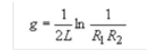
The animated emanation measure yields an expansion in photons as they travel along the waveguide. Joined with the waveguide misfortunes, invigorated emanation yields a net increase for each unit length, g. The quantity of photons can in this manner be kept up if the roundtrip enhancement in a hole of length, L, including the halfway reflection at the mirrors with reflectivity R1 and R2 approaches solidarity. This yields the accompanying lasing condition:

On the off chance that the roundtrip intensification is short of what one, the quantity of photons consistently diminishes. On the off chance that the roundtrip intensification is bigger than one, the quantity of photons increments as the photons travels to and fro in the pit. The increase needed for lasing hence approaches:
At first, the increase is negative if no current is implementing to the laser diode as ingestion overwhelms in the guidance of wave. As the laser current is expanded, the assimilation first reductions and the addition increments. The current for which the increase fulfills the lasing condition is the limit current of the laser, Ith. Underneath the limit current next to no light is radiated by the laser structure. For an applied current bigger than the edge current, the yield power, Mope, increments straightly with the implemented current, as each extra approaching electron-opening pair is changed over into an extra photon. The yield power in this way approaches:
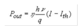
Where hν is the energy per photon. Figure 9 shows output power from a laser diode versus the applied current graph. The input, h, demonstrates that solitary a small amount of the produced photons add to the yield force of the laser as photons are halfway lost through the other mirror and all through the waveguide.

Figure 9: Output power from a laser diode versus the applied current.
Applications of optoelectronics devices
Optoelectronics is at the junction of gadgets and optics. Utilizing optical and electronic methods, it produces controls and converts light. Photonic gadgets measure, store, send and show data for applications like interchanges, shows, imaging, memory, bio photonics, energy age and lighting. Photonics is a fundamental piece of a country's data foundation, which, thusly, assumes a critical part in its homegrown economy and public guard.
The reason for this is to investigate uses of optoelectronics, with an accentuation on their business importance. This isn't an innovation audit, but instead a glance at the business effect of develops and arising optoelectronics advances.
In spite of the fact that PCs, purchaser hardware and correspondences are generally developed spaces of optoelectronics, they are in no way, shape or form stale. A constant flow of upgrades shows up in all sections. new advancements in a develop territory includes optical capacity. The advancement of optical stockpiling is guided by a diminishing spot size, empowered by diminishing the frequency of the chronicle laser bar. The size of an engaged laser bar is restricted by diffraction to a spot on the request for the frequency. Thus, the capacity thickness of optical stockpiling gadgets is conversely corresponding to the square of the laser frequency.
In Compact disc and blue ray players, infrared lasers are radiated onto the turning circle, where they "read" an example of infinitesimal pits that address the ones and zeros of advanced information. Supplanting the infrared laser with a more limited frequency elective permits a lot more modest pits and, therefore, considerably more information per plate.
As the frequency was diminished from the infrared of Albums to the red utilized in DVDs, stockpiling limit expanded by very nearly a significant degree. The 650-MB-per-side stockpiling limit of the Cd offered an ideal mode for music and voice, yet it couldn't oblige a full-length film. Consequently, the DVD was created with a limit of 4.7 GB per side, and it immediately turned into a business achievement, outperforming the development of albums.
1. LEDs could turn into the up and coming age of lighting and utilized anyplace like in sign lights, PC parts, clinical gadgets, watches, instrument boards, switches, fiber-optic correspondence, purchaser hardware, home devices, traffic lights, car brake lights, 7 fragment shows and latent presentations, and furthermore utilized in various electronic and electrical designing ventures, for example: Propeller Show of Message by Virtual LEDs, Driven Based Programmed Crisis Light, Mains Worked Drove Light, Show of Dialed Phone Numbers on Seven Section Show, Sun oriented Fueled Drove Streetlamp with Auto Power Control.
2.The sun oriented cells are relevant in provincial charge, media transmission frameworks, sea route helps, and electric force age in space and distant checking and control frameworks and furthermore utilized in various sunlight based energy based activities, for example: Sun based Energy Estimation Framework, Arduino based Sun powered Streetlamp, Sun oriented Controlled Auto Water system Framework, Sun oriented Force Charge Regulator, Sun Following Sun based Board, Sun powered based Undertaking from edgefxkits.com, Sun powered based Undertaking from edgefxkits.com
3. Photodiodes are utilized in numerous sorts of circuits and various applications like cameras, clinical instruments, and security types of gear, enterprises, specialized gadgets and mechanical supplies.
4.Optical strands are utilized in broadcast communications, sensors, fiber lasers, bio-medicals and in numerous different businesses.
5. The laser diodes are utilized in fiber optic correspondence, optical recollections, military applications, Cd players, surgeries, Neighbourhood, significant distance interchanges, optical recollections, fiber optic correspondences and in electrical undertakings like RF Controlled Mechanical Vehicle with Laser Pillar Plan, etc.
Consequently, this is about the optoelectronic gadgets which incorporate laser diodes, photograph diodes, sun powered cells, LEDs, optical fibers. These optoelectronic gadgets are utilized in various electronic venture units just as in broadcast communications, military administrations and in clinical applications.
Optoelectronic semiconductor gadgets have a significant effect on practically all spaces of Data Innovation. These gadgets can be grouped dependent on their useful jobs like yield, input, preparing, transmission, memory and others.
Numerous advances and actual properties are abused by applications utilizing Optoelectronics. A few such applications have gone to our agreement and control just during the earlier decade.
Beneath referenced are a portion of the utilizations of Optoelectronic gadgets:
1. Driven's have upset lighting framework and utilized in zones like PC segments, watches, clinical gadgets, fiber optic correspondence, switches, home devices, buyer hardware and 7 fragment.
2. Sun based Cells are utilized in a few sunlight based energy based ventures for estimation frameworks, auto water system framework, sun based force charge regulator, Arduino based sun powered streetlamps, and sun following sun oriented boards.
3. Optical Strands are utilized in telecom, fiber lasers, sensors, bio-medicals and different enterprises.
4. Laser Diodes discover their utilization in military applications, surgeries, optical recollections, Cd players, and neighbourhood and in electrical undertakings like RF controlled automated vehicles.
Optoelectronics is a fundamental establishment innovation that is empowering consistent working of the data business. Scholastically, Optoelectronics included the investigation of electronic a gadgets for transmission, discharge and tweak of light signals. Nonetheless, its degree has extended today and it incorporates electro-optics and photonics also. Financially critical advances for material science, correspondence, registering and medication are jumping on wards because of progressions in optoelectronics.
Optoelectronics innovation is giving greater scenes to Research and development today. Its impact can be found in the space of cost decrease, execution improvement and enormous volume producing. Modern and scholastic networks are foreseeing a splendid future for research in Optoelectronics Innovation. Progressing propels in Photonics and Optics is required to upset the 21st century.
Optoelectronic gadgets have consistently developed with new materials, advances, measure enhancement, furthermore, coordination for new employments. Their part in the public eye has gotten omnipresent by improving personal satisfaction and venturing into new applications for clinical, auto and purchaser hardware.
The most significant optoelectronic gadgets being used today and advance research on devices are being performed. It has examined how these gadgets were created dependent on profoundly inventive work which has changed semiconductor development innovation in the course of recent years. The prerequisites for leasing activity in semiconductors were examined just as the manners by which low-dimensional designs and strain might be utilized to improve the properties of gadgets like lasers (both edge-transmitting and surface-producing), modulators, speakers, and indicators. The part thought to be present status of-the-workmanship semiconductor laser gadgets and talked about arising future headings in semiconductor optoelectronic materials and gadgets. The optical correspondence is presently making its mark and is turning into the liked innovation in numerous applications. The incorporated electronic circuits have characterized the twentieth century as the hundred years of gadgets, while the 21st century is arising as the hundred years of photonics because of light wave innovation. The achievement of this advancement will prompt the improvement of new optoelectronic gadgets, a field where developments are advancing at "light speed".
Conflicts of interest: The authors declare that they have no conflict of interest.