Research & Reviews: Journal of Pure and Applied Physics
ISSN: 2320-2459
ISSN: 2320-2459
Dike UO*
Department of Pure and Applied Physics, College of Natural and Applied Sciences, Veritas University Abuja, Nigeria
Received date: 21/01/2020; Accepted date: 25/02/2020; Published date: 05/03/2020
Visit for more related articles at Research & Reviews: Journal of Pure and Applied Physics
Objective: Signal flow graph realization of higher-order current-mode all-pole low-pass current transfer functions with five Current Follower Transconductance Amplifiers (CFTAs) is presented. The fifth presented filters with one input and three outputs employ five CFTAs and five capacitors, and it can simultaneously realize third order low pass, fourth-order low pass, and fifth-order low pass current responses, from the proposed circuit topologies. Bipolar and CMOS technologies are used for CFTA implementation. This study aims to provide a literature survey for identifying research gaps and to design and implementation of the Current follower Transconductance Amplifier (CFTA) with constant gm demonstrated. To implement the CFTA active device in the bipolar technology structure depicted in CFTA which has been employed using transistor model parameters PR100N (PNP) and NP100N (NPN) of the bipolar arrays ALA400 and the COMS technology structure using, 0.5 μm CMOS process parameters for nMOS and pMOS transistors.
Methods: The approach had been based on drawing a signal flow graph directly from the given transfer function and then obtaining, from the graph, the Active-C filter involving CFTAs. Third-order Butterworth low-pass circuit requires only three CFTAs and three grounded capacitors, fourth-order Butterworth low-pass circuit requires only four CFTAs and four grounded capacitors and fifth-order Butterworth low-pass circuit require only five CFTAs and five grounded capacitors. One Filter based on input and output is characterized by its transfer function. The transfer function of a filter is the ratio of the output signal to that of the input signal as a function of the complex frequency. The obtained filter characteristics include the natural frequency (ωo) and the quality factor (Q-factor) which are electronically tuned through biasing current of the transconductance gain of the CFTAs. The resulting circuits obtained from the synthesis procedure are resistorless structures and are especially suitable for monolithic implementation. The circuits also have low sensitivity characteristics and exhibit electronic controllability coefficients via transconductance gains (gm) of CFTAs.
Results: To demonstrate the proposed approach, the third-order, fourthorder, and fifth Butterworth all-pole low-pass filters were designed and simulated using MATLAB Simulink. Conclusion: The study of the simulation of the third-order, fourth-order, and fifth-order all-pole low-pass filters has been carried out. The CFTA circuits have been simulated using MATLAB SIMULINK. The simulation results are in agreement with the theory.
Current follower transconductance amplifier (CFTA), Signal flow graph (SFG), Butterworth low pass filter and MATLAB simulink
The current Follower Transconductance Amplifier (CFTA) has been introduced in Biolek D [1]. This current input and output buildi ng block is particularly useful in realizing analog signal processing functions requiring explicit current outputs. The CFTA is slightly modified from the conventional Current Differencing Transconductance Amplifier (CDTA) [2] by replacing the current differencing unit with a current follower and complementing the circuit with a simple current mirror for copying the z-terminal current. CFTA is a composite of a CF usually realized from a translinear CCII, a Current Conveyor Transconductance Amplifier (CCTA) has directly a CCII followed by an OTA [3]. The CFTA element is a combination of the current follower and the multioutput operational transconductance amplifier. Consequently, there are several structures for realizing the current mode of active filters using CFTAs [4]. However, the work had been studied in the synthesis of the general nth-order all-pole lowpass transfer function. Also, the realization of an nth-order lowpass filter using current conveyors was introduced in Gunes EO [5] the circuit has too many grounded resistors, i.e. (n+1) current conveyors, n grounded resistors and n grounded capacitors. Therefore, this work largely focuses on presenting a general synthesis procedure for the realization of the Nth-Order all-pole low pass Transfer function. The approach is based on drawing a signal flow graph directly from the given transfer function and then obtaining, from the graph, the Active-C filter involving CFTAs. The resulting circuit uses a minimum number of n CFTAs and n grounded capacitors, which makes the circuit especially suitable for monolithic implementation. It is shown that the design procedure proposed here is general and simple. Simulation results from MATLAB Simulink illustrate the properties of the proposed design procedure.
In this present study, the recent work of Dike is extended to include the active building block Current Follower Transconductance Amplifier (CFTA) and its basic applications like amplifiers, grounded and floating inductors and active filters in analog signal processing. Designed examples and computer simulations by Matlab Simulink confirm the usefulness of the proposed approach. Its various instrumental applications are filter and conventional controllers (proportional, integral and derivative). These CFTA based conventional controllers are studied and their characteristics are analysed through computer simulation and verified in Matlab Simulink.
Literature Review
Bipolar and CMOS technologies are used for CFTA implementation. One of the CFTA realizations using bipolar technology is reported in Herencsar N [6]. The advantage of these circuits is high overall gain compared to CMOS based implementations. A high gain, these CFTA structures also produce high power dissipation due to the use of leakages in BJT. Another bipolar implementation which is an extension of CFTA known as ZC-CFTA is presented in Tangsrirat W [7]. In this structure, an extra z-terminal termed as z-copy is included to provide design flexibility. A Current-Controlled CFTA (CCCFTA) based on BJT technology is presented in Jaikla W [8]. In this structure, the input voltages of f-terminals is zero and therefore these terminals have a finite resistance that can be controlled through bias currents [9-11].
CMOS is also sometimes referred to as complementary-symmetry metal-oxide-semiconductor. The words “complementarysymmetry” refer to the fact that the typical digital design style with CMOS uses complementary and symmetrical pairs of p-type (PMOS) and n-type (NMOS) metal oxide semiconductor field-effect transistors (MOSFETs) for logic functions. CMOS technologybased CFTA structures has also been reported in the literature. One such structure is reported in Chauhan AS [11] which has an advantage of high impedance at the z-terminal. A low power CMOS realization of the CFTA is reported in Li YA [12]. In this structure, the input stages are constructed using FVF, due to which this CFTA has very low input resistance. The modification of CFTA known as CC-CFTA is reported in Herencsar N [3] which has the advantage of better OTA gain and multiple outputs can be drawn out of CFTA. Another CMOS based CFTA is reported in Herencsar N [13]. This circuit exhibit very low impedance at the inputs and high (typically in GΩ). A comparison of available CFTA structures in terms of supply voltage, technology and number of transistors, gain, power dissipation, and terminal impedances is presented in Table 1.
| Reference | Technology | Supply voltage | Bais current | Transconductance gain | Power dissipation |
|---|---|---|---|---|---|
| Tangsirat et al. | Bipolar | ± 3 V | 100 μA | 2 mS | - |
| Lahiri et al. | Bipolar | ± 2.5 V | 50 μA | 0.96 mS | - |
| Jaikla et al. | Bipolar | ± 1.5 V | 100 μA | - | 8.11 mW |
| Tangsrirat et al. | 0.35 μCOMS | ± 2.5 V | 10 μA | - | 0.43 mW |
| Herencsar et al. | 0.5 μCOMS | ± 1.85 V | 400 μA | - | 10.6 mW |
| Singh et al. | 0.25 μCOMS | ± 0.75 V | 40 μA | 0.6 mW |
Table 1. Bipolar realization of CFTA
Bipolar realization of the CFTA used in this work is shown in Figure 1. The circuit consists of a current conveyor circuit Q1- Q8 and operational transconductance amplifier Q9-Q20. Therefore, in this case, the transconductance gain 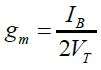 is directly proportional to the external bias current IB, which can be written as where
 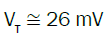 at 27°C is the thermal voltage.

Figure 1: Bipolar realization of the CFTA.
CMOS Realization of CFTA
CMOS-based CFTA circuit realization suitable for the monolithic IC fabrication is displayed in Figure 2.

Figure 2: CMOS realization of the CFTA.
CMOS realization of the CFTA used in this work is shown in Figure 2. The circuit consists of a current conveyor circuit Q1- Q8 and operational transconductance amplifier Q9-Q20. Therefore, in this case, the transconductance gain of CMOS based 1th CFTA (i=1,2,3), can be controlled through the biasing current IBi which can be written as 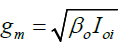 where
where 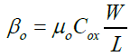 is the process parameter, is the free electron mobility in the channel, is the gate oxide capacitance per unit area, W and L are the channel width and length respectively.
In the past few decades, the current mode (CM) analog signal processing has received considerable interest owing to the advantages offered by CM techniques which have been elaborated. This has resulted in the emergence of various CM analog building blocks and CFTA is one among those. The CFTA block was first reported by Biolek D [2]. A Current Follower Transconductance Amplifier (CFTA) can be considered to be a reduced version of the CDTA instead of the current-differencing unit as the front end, it has a current follower as the front end which can be easily implemented from a CCII+ by grounding its Y-terminal. The operation of the CCII current conveyor is such that if Current conveyor (CCII+) is constructed by a Voltage Follower (VF) between the Y-terminal and the X-terminal in order to accomplish vx=vy, and a Current Mirror (CM) between the X-terminal and the Z-terminal in order to accomplish iz=ix [14]. The block diagram of the CFTA can be drawn as shown in Figure 3a. Thus, it is a four-terminal building block having one input terminal f and three outputs terminals Z, x+ and x-. The output current entering into terminal Z is the same as the one entering into the low impedance terminal f, whereas when terminal Z is terminated into an impedance, two complimentary output currents are available as i+x and i-x which are respectively given by i+x =gmvz and i-x =-gmvz. A CC-based implementation of the CFTA is shown in Figure 3b which can also be considered to be a special case of the CDTA with input terminal n being grounded [12].

Figure 3: CFTA realization (a): block diagram implementation; (b): Implementation of the CFTA using CCII and OTA.
This current input and output building block is particularly useful in realizing analog signal processing functions requiring explicit current outputs. The symbolic representation of the CFTA and its behavior model are shown in Figure 4. Assuming the standard notation, the terminal defining relations of this device can be characterized by the following set of equations [4].

Figure 4: The CFTA.